
Building a “$5 Forth Computer” – First Steps
This week I have been designing a tiny 16-bit computer around a FRAM based MSP430 microcontroller. The MSP430 is well known for low power, and at 16MHz will outperform an Arduino by a factor of 4. Coupled with the non volatile Ferro-Electric RAM – or FRAM, which is not only much lower power and faster than flash, it can be used like RAM. A controller that can survive a power failure and then start up when the power returns – with no loss of data.
I decided that I wanted something that could execute the Forth language efficiently, and so the 16 bit MSP430 is almost ideal. It's an uncomplicated little processor with a neat way of bootloading it through a serial connection. It's a nice fit with my desire to make a “Neo-Retro” compute module which can execute code from external memory using a virtual Forth Stack Machine.
“Neo – Retro” is the new kid in town around hobbyist tech projects. It's the attempt to recreate machines of bygone eras, using up to date hardware, such as FPGAs. Closely related to retro-gaming, the challenge is to prove just how much you can do with limited resources. This ChipStick module, described in an earlier post, is just the first part of an on-going project to recreate a complete 80's era machine – in 4 chips or fewer.
As a historical aside, in the early 1960s – the 12 bit PDP-5 was the forerunner of the PDP-8, which set the scene for the next decade of minicomputer development. The PDP-5 was housed in a 72″ cabinet yet only had 4K words of memory and a 6uS memory cycle time. The 4mm square IC at the heart of the ChipStick exceeds the speed of the PDP-5 by a factor of 100 times and could emulate the PDP-5 in real time and act as a virtual machine – executing code from the external SRAM. The PDP- cost $27,000 back in '63. I paid about $2.70 each for the 20 sample processors I just purchased from TI.
If you just got here – here's the story so far:
In Sunday's Post I illustrated the EagleCAD for the pcb for this new module. These tiny boards will be back from the manufacturer by the middle of next week, in time for a long weekend over Easter. They have been designed so that four will fit onto a 50 x 50 mm board, thus keeping manufacturing costs down. If anyone reading this knows how to panelise gerbers or EagleCAD files – I'd be interesting in hearing from you.
The intention is to release these boards as an open source design, and possibly run a Kickstarter to fund the manufacturing of a 1000+ batch. I'd like to think that $5 was achievable with volume production.
These modules are like sticks of gum, you buy 4 or more in a pack and then you just use them as required to provide the intelligence for small projects. See my earlier post on “Nano-Computing”.
On Tuesday – I outlined the concept of The $5 Forth Computer – whilst waiting for the ICs to arrive from the US. They turned up first thing on Wednesday, with the IC prototyping boards arriving on Thursday. It looks like it's going to be another busy week for Solomon Grundy.
And now putting theory into practice. In this post we look at a new MSP430 FRAM based device – the MSP430FR2433. It has 15K of FRAM, 0.5K of Info FRAM and 4K bytes of SRAM. As well as the memory, there are 3 serial communications interfaces, a multichannel 10 bit ADC and 3 timers. All of this, in a tiny low cost package – which makes for an almost perfect breadboardable Forth Computer.
The MSP430FR2433 from Texas Instruments costs about $1.36 in volume – and $2.58 in 1 off. It is not yet in full production (early June) – but samples and small quantitiescan be ordered from TI's online store.
With a little creative design, low cost parts and a tiny 2 layer pcb we are en-route to offering a Forth Computer which could cost as little as $5 when produced in volume.
In this first part we look at the process of creating a prototype – and the practical challenges of dealing with a chip that is just 4mm x 4mm. I then discuss how to program the code onto this prototype.
I have chosen to summarise the main points here – what I don't mention is the 12 hours of angst, trying to program the device with an incompatible programmer!
Mounting the IC on a PCB.
The MSP430FR2433 is available from TI's online store as a 24 pin QFN in a 4mm square package. This immediately opens up some challenges for the home constructor – but fortunately there are a couple of prototyping products that make soldering this chip down and using on a breadboard a lot easier.
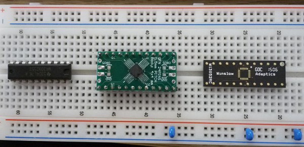
On the left we have the usual MSP430G2553 for size comparison. In the middle is the Schmartboard QFN adaptor ($6) and on the right the $10 Winslow Adaptics product. There are other manufacturers of equivalent products – including Aries, Roth Electronik, Proto-Advantage – but the challenge was to get the right pin pitch of 0.5mm at short notice. Below are the two products in greater detail.
The Winslow Adaptics part is the smaller of the two reviewed with an 0.3″ overall width – so it's the same width as a standard DIL package. The carrier board has gold flashed traces, for corrosion resistance and easier soldering. The pins are turned pin – so they will fit into standard IC sockets – and are also gold flashed. This is a quality product – but I ended up paying about $16 each for these – once purchase tax and shipping had been added. In the UK RS Components stock them – and in the US – they have a US Sales office:
Winslow Adaptics Inc
Rocky Point Centre
3001 N.Rocky Point Drive East
Suite 200
Tampa, FL 33607
Toll Free: 1-866-WINSLOW
Fax: 941 483 3209
The Schmartboard is a cheaper product and comes as a kit with a pin header that you solder in yourself. Schmartboard have an innovative solution for ensuring soldering success – described here.
You will need a very fine soldering iron – with a point tip, and SMT soldering flux. I suggest you read the supplied instructions first – as the approach is quite different to the usual manual soldering method. Note that the pin spacing is 0.5″ on this product.
In my opinion the Winslow product was the easier to use, for someone who regulary solders down small SMT packages. The Schmartboard may have been more appropriate for LQFP packages – but didn't really make soldering the QFN any easier. Perhaps once I have practiced on a few, things may be easier!
That's the hard bit over!
Once the device has been soldered onto the prototyping adaptor, the device pinout can be reviewed. The following diagram shows the pinout – assuming that you have aligned pin 1 of the package in the correct location. This is an easy mistake to make. The markings on the sample chips were difficult to read – even with magnification.
+———U———-+
/RST | 1 24 | DVCC
TEST | 2 23 | DVSS
UCA0 TX | 3 22 | XIN
UCA0 RX | 4 21 | XOUT
UCA0 CLK | 5 20 | P3.2
UCA0 STE | 6 19 | P2.7
UCB0 STE | 7 18 | DVSS
UCB0 CLK | 8 17 | UCA1 TX
UCB0 MOSI | 9 16 | UCA1 RX
UCB0 MISO | 10 15 | UCA1 CLK
P2.2 | 11 14 | UCA1 STE
P3.0 | 12 13 | P2.3
+——————–+
Notes on Pin Out
It should be noted how neatly the pinout gives access to the three separate communications peripherals UCA0, UCA1 and UCB0 present on the MSP430FR2433.
The 6 pins needed to provide the UART based Boot Loader (BSL) are conveniently all together and at the top of the IC on pins 23, 24, 1, 2, 3 & 4.
If the 32kHz crystal is not needed – then Xin and Xout provide a further two GPIO lines
The MSP430FR2433 provides up to 12 channels of 10 bit ADC.
Wiring it Up
For the initial programming we use Spy By Wire or SBW programming. This uses a Launchpad MSP430FR4133 device to act as the programmer – with the harness using just 4 wires. Connect it up with jumper wires using the following steps:
1. On the Launchpad, locate the 18 way (2×9) connector J101. Remove the jumper links on 0V, SBWTDIO and SBWTCK.
2. Connect SBWTCK to pin 2 (TEST) of the module.
3. Connect SBWTDIO to pin 1 (RESET) of the module.
4. Using a jumper wire connect pin 18 to pin 23 of the module – links the DVSS pins
4. Connect 3V3 to pin 24 of the module
5. Connect 0V GND to pin 23 of the module
6. Connect a LED via a 270R resistor to P1.0 (pin 7) of the module. The cathode of the LED should go to 0V
No other connections are needed. See the diagram below:
+———U———-+
SBWTDIO ->> /RST | 1 24 | DVCC ->> 3V3
SBWTCK ->> TEST | 2 23 | DVSS ->> 0V
UCA0 TX | 3 22 | XIN
UCA0 RX | 4 21 | XOUT
UCA0 CLK | 5 20 | P3.2
UCA0 STE | 6 19 | P2.7
LED/270R>> UCB0 STE | 7 18 | DVSS ->> 0V
UCB0 CLK | 8 17 | UCA1 TX
UCB0 MOSI | 9 16 | UCA1 RX
UCB0 MISO | 10 15 | UCA1 CLK
P2.2 | 11 14 | UCA1 STE
P3.0 | 12 13 | P2.3
+——————–+
The MSP430FR2xxx series is very similar to the MSP430FR4xxx series – so the integral FET programmer on the Launchpad will recognise the ‘2433 device, and after retrieving new programming firmware update will program it. I used the TI Code Composer Studio (CCS) to write the Blinking LED sketch.
With 32Kbyte SPI SRAM attached and executing code as a virtual Forth Machine from RAM.
PCB Designs
I use EagleCAD for most of my pcb work – partly because it has a great community behind it, and a wealth of device footprint libraries are available from Sparkfun, Adafruit, Seeed and Farnell/Element 14.
Now that the concept of MSP430 plus an external SRAM or FRAM chip has been proven, it is time to consider other pcb formats that may be useful to the community. Last week I laid out the 20 pin DIL version “ChipStick” – which is the entry level G2 Launchpad compatible version. This weekend I have looked at other alternatives, based on the same circuitry SPI memory plus MSP430 as a plug in module:
For More Details: Building a “$5 Forth computer”