
Designing a Mains Frequency Monitor, Part 2
This is the second in a series of posts about designing a mains frequency monitor using the Microchip PIC 16F1619 microcontroller. In this post we will take a look at the first revision of the board that I designed for the project and some of the features that it adds.
Be sure to read Part 1 of the project write-up if you haven't done so already.
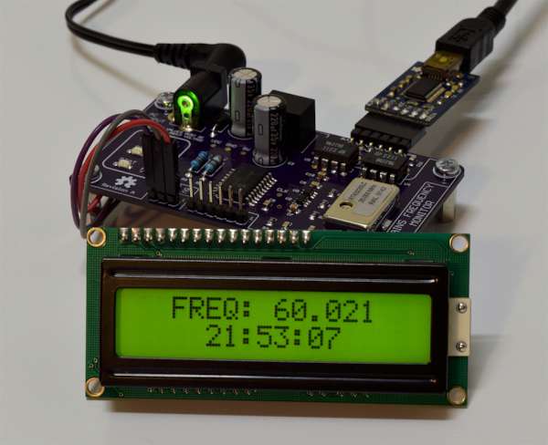
First revision of the Mains Frequency Monitor board.
PCB Progress
I designed a PCB for this project a couple of weeks ago, and recently received the boards back from OSHPark. I think it turned out great! The board houses the microcontroller and 20MHz TCXO that we discussed in Part 1. For the power supply I opted for a Recom DC-DC converter to generate 5V from the rectified input from a 12V AC wall adapter. There is a programming port (PicKit3 compatible) for programming the microcontroller as well as a header to hook up the LCD.
I also added an opto-isolated terminal port that is compatible with common Serial-to-USB adapters such as the FTDI Friend, FTDI Basic Breakout, and all of the various clones available online. This is nice for capturing data in a log file and then analyzing it in a program such as TimeLab.
The PIC 16F1619 only has one USART, but I wanted to use the same serial LCD display I have been working with throughout the prototyping phase. I also needed the USART for the terminal interface. To get around this I added a SPDT analog switch (74LVC1G3157) to allow sharing of the USART with both ports. The serial LCD only needs the Tx line, so the Rx line from the USART connects directly to the terminal port.
The Mains Frequency Monitor has three ports: programming, Serial LCD,
and an opto-isolated terminal port for data logging.
Here's a short video showing two of the boards in operation:
Performance
With assembled PCBs to test, I have been able to collect some data. Here is a frequency difference plot in TimeLab for a 12 hour run:
Mains Frequency, 12 Hour Run, Frequency Difference
And here is the ADEV plot for the same run:
Mains Frequency, 12 Hour Run, ADEV
Much longer runs will be required in the future. Also, I plan to rig up a test with the board and a proper frequency counter measuring the same signal to allow for a good assessment of the board's performance. I've done some informal comparisons with a calibrated counter and I'm very confident in the accuracy of the readings from the board.
Design Files
I plan to wait until the project is finished before creating a project link on OSHPark, publishing the BOM, etc. Rev A of the board is working out well, but it might still be necessary to make some changes. Don't worry, everything will be shared and documented fully in Part 3 when we wrap up. For now, the design files are available in the GitHub repo if you would like to check them out. I have also updated the firmware version in the repo.
Here's the schematic of Revision A:
For More Details: Designing a mains frequency monitor