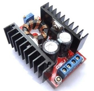
In a recent project, I needed a boost converter to step up 5V to about 8V at a few amps. A few different Chinese-made boost converter modules are available from various sources: I’ve seen them on eBay and Amazon. One very common one is known as the ‘150W Boost Converter’. I believe it’s intended for charging laptops from car batteries. It’s specified to take an input of 10-32V and output 12-35V, which isn’t quite what I was looking for, but the price was right so I thought I’d take a chance. This is what I found.

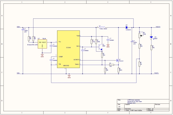
It’s a pretty straightforward boost converter topology with a MOSFET switching transistor and a variable resistor in the feedback loop to set the output voltage. There is no over-current, over-voltage or reverse polarity protection at all, and the chip isn’t designed for low power consumption so this module wouldn’t be suitable where very low standby power is a requirement. There are a couple of interesting features, though.
The circuit includes an arrangement with an NPN transistor which feeds some bias to the current sense feedback loop. According to the UC3843 datasheet, this improves the stability of the converter at duty cycles higher than 50%.
The control supply for the UC3843 is derived from a 9V regulator, so it’s independent of the input or output voltage. This is convenient.
The UC3843 is designed to operate from fairly high supply voltages, and won’t start up until its supply voltage reaches 8.4V. That was a bit of a problem for my application, where the input voltage was only 5V. However, there’s nothing to say that the chip power supply has to be the same as the power input. In fact, the module already has a handy 9V regulator which feeds the control chip. Looking at the circuit diagram, there are even a pair of resistors (I’ve labelled them R1 and R2) which select whether that regulator is fed from the input or the output. As supplied, R2 was fitted, so the control chip was fed from the output. Here’s a closeup of the relevant part of the board showing R1 and R2.
For more detail: 150W Boost Converter Schematic


