
Digital design refers to creating digital circuits. Digital circuits are in basically everything today and range from something as simple as a circuit that turns an LED on when a button is pressed to the complex processor in the device you are reading this on. Traditionally, these circuits are built by making ASICs (Application Specific Integrated Circuits) out of silicon wafers. This process is incredibly expensive and complex.
FPGAs, or Field Programmable Gate Arrays, are a way to create digital circuits without these barriers. FPGAs are part of a class of devices known as programmable hardware. This means that you can design a digital circuit and program the FPGA to become that circuit. You can reconfigure the FPGA as many times as you want allowing you to create circuit after circuit without having to physically change a thing!
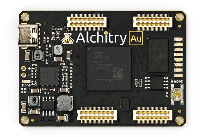
This time around, there are two FPGA boards! These are the Alchity Au (gold) and the Alchitry Cu (copper).
Specifications
- Artix 7 XC7A35T-1C – 33,280 logic cells (approx. 4x the capacity of the Mojo)
- 256MB DDR3 RAM
- 102 IO pins (3.3V logic level, 20 of then can be switched to 1.8V for LVDS)
- 9 differential analog inputs (1 dedicated, 8 mixed with digital IO)
- USB C to configure and power the board
- 8 general purpose LEDs
- 1 button (typically used as a reset)
- 100 MHz on-board clock (can be multiplied internally by the FPGA)
- Powered with 5V through USB C port, 0.1″ holes, or headers
- USB to serial interface for data transfer (up to 12Mbaud)
- Dimensions of 65mm x 45mm
The Alchitry Au is the workhorse of the two boards. It features an Artix 7 FPGA which means no more dealing with Xilinx’s antiquated ISE tool. This board also has 256MB of DDR3 RAM while still having 102 IO pins available for your projects!
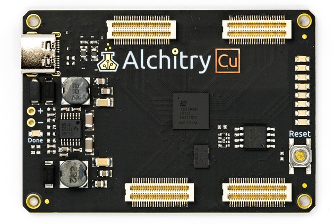
- CE40-HX8K FPGA – 7680 logic elements (approx. 0.8x the capacity of the Mojo)
- 79 IO pins (3.3V logic level)
- USB C to configure and power the board
- 8 general purpose LEDs
- 1 button (typically used as a reset)
- 100 MHz on-board clock (can be multiplied internally by the FPGA)
- Powered with 5V through USB C port, 0.1″ holes, or headers
- USB to serial interface for data transfer (up to 12Mbaud)
- Dimensions of 65mm x 45mm
The Cu board is the lighter version of the two but offers something completely unique. The Cu uses a Lattice iCE40 HX FPGA that is supported by the open source tool chain Project IceStorm. The Mojo IDE will be transformed into Alchitry Labs to support the new boards. Alchitry Labs will be open source meaning that the Alchitry Cu can be developed for using entirely open source tools!