
Problem Statement
1.1 Requirements and Specifications
Due to the system being a completely new idea, specific requirements were not provided. It was decided
that the following values should suffice for an efficient system. The group will strive to meet all of the
following quantified expectations:
● Objective/Purpose: The main requirement is to effectively filter contaminants within a liquid.
This will be accomplished by using a 0.2 µm polyvinylidene difluoride (PVDF) membrane.
● Low Maintenance: The idea of the system is to utilize a self-cleaning filter membrane.
Therefore, the system should be able to clean the membrane and regain its permeability to 75-
100%.
● Ease of Use: The operation of the system should not be difficult to learn since the ultimate goal
of the design would be to incorporate it worldwide. The time required to learn the operation the
system should be under 60 minutes.
● Universal Operation: The system should be powered with a standard AC 120v source. This will
ensure that it can be used in most areas without further hardware.
1.2 Given Parameters
The given parameters are to be accounted for designing this filter system. Certain parameters can be
changed upon further experimentation. The following are the given parameters:
PVDF Membrane:
● The PVDF membrane is a .2 µm-pore sized microfiltration membrane supplied by Dr. Dong
Chen.
● The PVDF membrane will be poled using a minimum of temperature of 85 °C in the oven.
● The permeability of the membrane will be examined by filtration of 1 mM KCI solution at 34.5
kPa gauge pressure.
Signal Output System:
● The signal output system will provide amplitudes in the range of 0-25V.
● The outputted frequency should be adjustable from 10 Hz to 600 kHz.
● The functions should at least have sinusoidal and square waveforms.
Membrane Filtration System:
● Membrane Filtration System that we’ll be using is defined to be a single pipe that the membrane
will be found in with no feedback.
1.3 Design Variables
The system that we are developing has many design parameters that must be met, yet there is still
variability within this project. Most of these variables are processed based rather than hardware based
therefore these variations are categorized into two distinct categories which will be Electrical and
Mechanical Variables.
Electrical Variables:
● Poling Variables: The electrical poling is the process of sending an electric field through the
filter aligning the poles of the atoms thus making the filter have piezoelectric properties. Varying
the duration of the poling potential difference and the amplitude of the potential difference will
affect the degree of poling.
● Signal Output System: The signal output system that needs to be designed is a variable in itself.
The hardware is to be determined to obtain the parameters that were given.
● Membrane Vibration Measurements: The vibration of the membrane will have to be recorded
using a type of high frequency measurement system. This system should be able to record the
frequency of the membrane and display the results for spectral analysis purposes during testing.
● Data Collection: The vibration measurements are to be sampled and stored for future use. The
data could then be read for optimization using readily available or design software.
Mechanical Variables
● Filtration Pressure: The filtration process with the piezoelectric membrane will be operated at
varied filtration pressures (e.g. from 6.9 to 34.5 kPa).
● Fluid Content: The fluid content that will be filtered will have a play in this system. The
contamination of the supply and the flow rate will affect how the filter operates.
1.4 Limitations & Constraints
The filtration system itself has been designed by Dr. Chen and is stationed in the IPFW Environmental
Engineering Laboratory. The limitations and constraints placed on our designs are specifications that need
to be met in order for our designs to be able to work in collaboration with Dr. Chen’s original idea.
● High Voltage Power Supply: The polyvinylidene difluoride (PVDF) membrane must be put
through a polling process to generate a magnetic field and ready the membrane for vibration. The
maximum voltage that can be supplied is 20kV.
● Maximum Polling Voltage: During the poling process, there is a maximum polling voltage value
for the type of membrane we will be using. Any voltage above this value will not increase the
polarity and could cause arcing, short circuiting, and damage to the membrane.
● Budget: The cost limitation of our design project is around $1,000.
1.5 Other Considerations
The following are design considerations not mentioned above. The conceptual design will utilize these
ideas even though they were not specifically required:
● Programmable User Interface: User should have the control to select how many days per week
and what time during the day the system will automatically operate (e.g. 12:00AM, 3:00AM).
This feature should be user friendly and have the option to be set to recommended settings.
● Wireless Capabilities: The data that is collected from the vibration measurement device could be
transmitted wirelessly to a phone app or laptop software.
The Detailed Design
2.1 Functional Overview of System
2.1.1 Overall Overview
Throughout the designing of the piezoelectric membrane filtration system, the given parameters,
design constraints, and the requirements were considered when designing the system.
Specifications of the signal output system, data collection, data analysis, data storage, user
interface, and the measurement device were the main focus of the design process.
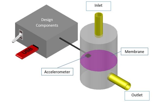
As shown in Figure 1, the system of all of the functioning components will be placed in a single
box. The box will have a simple on switch for the user to operate the system. A USB port will
also be found to connect a drive for data to be stored onto for later analysis. Wires will connect
the components in the box to the vibration measurement device and the piezoelectric membrane
filter.
2.2 Signal Output System
The signal output power system will consist of three pieces which are the Raspberry Pi controlled output
system, amplifying circuit, and voltage supply. Designing this system we need to make sure that all of our
specifications in terms of frequency, amplitude, and waveform are met.
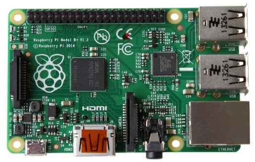
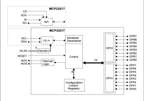
2.2.1 Raspberry Pi Controlled Output System
This system is comprised of three parts which are the Raspberry Pi microcontroller, and the
AD9850 DDS module. The Raspberry Pi 2 Model B is a powerful microcontroller. It carries a
900 MHz quad-core ARM Cortex A7 CPU along with 1GB of RAM. It is equipped with 4 USB
ports, 40 GPIO pins, Micro SD card slot, I²C interface as well as SPI and other features. This
microcontroller will be used to send information to the AD9850 DDS via parallel communication
using the GPIO ports of the microcontroller.
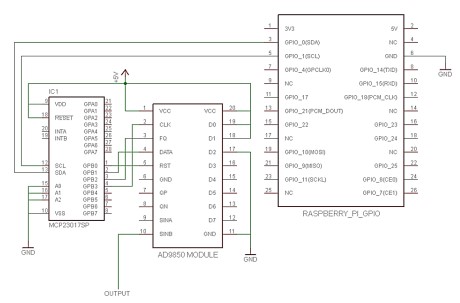
The MCP23017 is a 16-bit I/O expander with serial interface. The I/O pins are controlled by a
system master which determines whether the pins will be used as input or output. The information
is read from the I²C serial bus and into the control of the 16 I/O pins. In our system, we will
control 4 of the 16 I/O pins to send information to the AD9850 DDS.
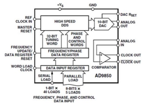
The AD9850 is a powerful DDS module. This module includes a comparator, high-speed digital
to analog converter and high frequency internal crystal which together provide the tools to create
a digitally programmable frequency synthesizer and clock generator. Some of the features of this
module include a 125 MHz internal clock, DAC SFDR > 50 dB at 40 MHz analog output, 32-bit
tuning frequency tuning word, and a control option of either parallel or serial byte loading format.
The maximum output frequency of this module is half of the internal clock speed, 62.5 MHz,
which satisfies our frequency needs.
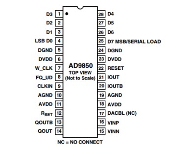
The 4 outputs pins being controlled on the MCP23017 with control the pins 7,8,12, and
25 on the AD9850. Pin 7 controls the word clock, this pin is used to control the loading
of the serial data. Pin 8 controls the frequency of the output, the frequency is updated on
every rising edge of the clock cycle. Pin 12 is the DAC external reset which controls the
DAC full-scale output analog output current. Pin 25 is the MSB of the parallel load or in
this case the serial data loading pin. Pin 21 is the analog output of the DAC which will
give the final output.
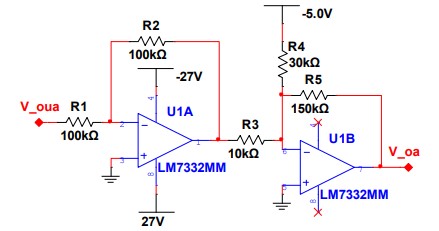
2.2.2 Amplifier System
The output voltage of the AD9850 DDS is between 0 and 3.3V which is not within the required
range therefore an amplifying circuit will be built to rectify this problem. No DC offset is desired
therefore this must be removed and also the max amplitude of the output signal is 25V so this
must be accounted for which is described in equation (1).
??,?
(?) = ?? ⋅ (??,??(?) − ???) (1)
??,?
(?): Output voltage post amplification
??: Gain of the system
??,??(?): Unamplified output voltage
???: DC offset of the output voltage
The DC offset can be solved by averaging the maximum and minimum output values as seen in
equation (2).
??? =
?? ?(??,??) + ?? ?(??,??)
2
3.3? + 0?
2
= 1.65?
(2)
The gain of the system can by solving for the Ag
term by putting the upper limits of the desired
output voltage and the highest possible input voltage, which is solved for in equation (4).
?? ?(??,?) = ?? ⋅ (?? ?(??,??) − ???) (3)
?? =
?? ?(??,?)
?? ?(??,??) − ???
25 ?
3.3? −
3.3?
2
= 15.15 ≈ 15 (4)
The characteristics the operational amplifier are then represented in the circuit, as seen in Figure
8.
The first operational amplifier is merely an inverting operational amplifier that is also used to
isolate the Raspberry Pi from the rest of the circuit so 100 kΩ Resist for both R1 and R2 to not
only have a unity gain but also to keep the power consumed by these resistors low. The second
operational amplifier and R3, R4, R5 and VRef uses a summing amplifier set up to not only add in
the positive DC component to the inverted unamped voltage supply, thus removing said DC
component from the unamped voltage supply, but also to amplify the ac component. The removal
of the DC is relatively simple, since the DC current through R3 can be described by iDC = VDC ÷
R3then VRef ÷ R4 must be the same, therefore the ratio of R3/R4 can be found, as seen in
equations (6).
??? =
???
?3
????
?4
(5)
?4
?3
????
???
(6)
Since there are two unknowns in this equation we can arbitrarily set one variable and solve for the
other so assuming 100 kΩ we can solve for R4 as seen in equation (7).
?4 = ?3 ⋅
????
???
= 10 ?? ⋅
5?
3.3? ÷ 2
= 30.30?? ≈ 30?? (7)
The gain of the AC component of purely resistance operational amplifier can be described in
equation (8), therefore R5 can be solved for as seen in equation (9).
?? =
?5
?3
(8)
?5 = ?? ⋅ ?3 = 15 ⋅ 10 ?? = 150?? (9)
The LM 7332 operational amplifiers were chosen for this design because they are widely many
application, cheap and efficient for getting this task done. These operational amplifiers can work
up to ±30V. Therefore it can work under our voltage supplied as calculated in section 4.2.3. The
figure below shows the operational amplifying system that be used with all proper components.
calculated in the equations above
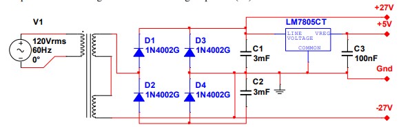
2.2.3 System Voltage Supply
In order to run the equipment specific voltage levels must be created to supply the right power to
the devices. One of the simplest ways to provide more than ±25 V was using a center tapped
transformer rectifier, 4 diodes, and 2 capacitors to create a full wave rectifier, as seen in Figure
- A 2:1 center tapped transformer is used to decrease the rectified output voltage. The DC
component of the voltage can be found through equation (11).
??? =
1
? ⋅ ?
∫ ????√2?? ? ? ??
?
0
(10)
?: Winding ratio of the transformer.
???: The DC component of the rectified circuit
????: The root mean square of the voltage, for this instance it’s
120 V
??? =
2
3
2
⁄
⋅ ????
??
2
3
2
⁄
⋅ 120 ?
2 ⋅ ?
= 54.02 ? (11)
Since half of the potential difference is over the positive to neutral lead and the other half is over
the neutral to negative lead, the positive voltage supply will be 54.02 V÷2= 27.01 V. The
capacitors are used to decrease the ripple voltage across the output voltage. Equation (12-13)
describes the ripple voltage across an RC circuit. Since the equivalent resistance across system
will be high, a 1 kΩ will be used to simulate the resistance of the system.
Source: Design, Fabrication, and Testing of a Piezoelectric Membrane Filter System