
Introduction
1.1 Motivation
On August 14, 2003, North America suffered its largest blackout. Major 345 kV transmission lines dropped out of service, unbeknownst to operators, causing a cascading outage that extended across the Midwest, Northeast, and into Canada [1]. An investigation launched by the North American Electric Reliability Corporation (NERC) found that the blackout could have been confined to a small region had operators known the status of overstressed and failing lines [2].
Since this catastrophe, steps have been taken to improve real-time, networked monitoring of America’s electrical transmission and distribution network, in order to enable
system operators to predict and counteract or confine disturbances. Increased situational
awareness can also allow the dynamic calculation of maximum load ratings based on environmental conditions. Overall, improved monitoring allows utilities to provide power to
customers in a more efficient, more reliable, and safer way.
The installation of phasor measurement units (PMUs) provides a real time image of
operating conditions. Increasing the number of PMUs improves the resolution of data
available to control room operators. It also creates the possibility for implementation of
automatic control systems to correct disturbances or failures. However, these devices are
costly, approximately $43,400 per installation, and are hard to install [3]. They also require
dedicated communication networks to feed data back to centralized processors, known as
phasor data concentrators (PDCs).
PMUs can offer a new insight when installed at the distribution level of the power grid.
The prevalence of distributed generation, smaller power plants that supply communities
rather than regions, is increasing due to the fact that renewable power generation is better
suited for communities. This increase causes an increase in dynamic events at the distribution level, as wind turbines and solar farms increase and decrease their output in step with
the weather. Having PMUs measuring at the distribution level will give a more accurate
picture of how the increase in distributed generation affects the power grid on a day-to-day
and long term basis.
1.2 Objective
The goal of this project is to design a low cost PMU that takes measurements at the
residential level of the power grid. This device should be easy to manufacture and highly
reliable. It should communicate results back to a central database using the protocol
described in the IEEE Standard for Syncrophasor Data Transmission.
Background
2.1 Synchrophasor Definition
Alternating Current (AC) is mathematically represented by a cosine wave,
x = A cos(2πfACt + φ) (2.1)
where fAC = 60Hz in North America. Using a technique proposed by Charles Proteus
Steinmetz in [4], AC can be represented as a simplified quantity called a phasor. When
representing a cosine as a phasor, it is assumed that the frequency of the signal remains
the same. Therefore, the variable quantities are magnitude and phase. For AC, magnitude
is commonly defined as the root mean square of voltage. Equation (2.1) becomes
X =
A
√
2
φ (2.2)
Establishing phase requires either a signal or time reference. Synchrophasors calculate
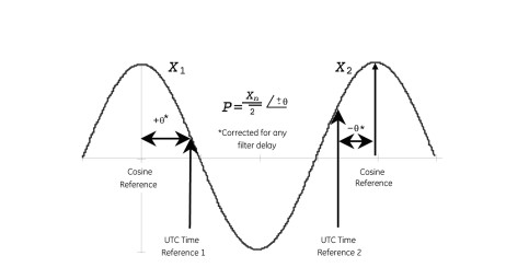
phase using an absolute time reference, commonly Coordinated Universal Time (UTC). Figure 2.1 shows a cosine superimposed on a UTC time pulse. The synchrophasor is defined
to be 0◦ if the cosine has a maximum during the pulse and 90◦ if the cosine has a zero crossing at the pulse. Values between 0◦ and 90◦ are calculated according to the selected phasor estimation algorithm [5]. Previously, phasor measurement at generators and nodes in the transmission network was impractical due to geographic separation between the two. Implementation of synchrophasors allows for easy calculation of magnitude and phase differences between nodes based off a shared standard time.
2.2 Previous Work
The concept of a synchrophasor was first introduced in the 1980s and has since generated
a large body of commercial and academic research. It is impossible to address all work
on synchrophasors and their applications in the scope of this project so emphasis will be
placed on development of inexpensive PMUs.
K. Kirihara, B. Pinte, and A. Yoon designed and tested a relatively low cost (approximately $1050) PMU as part of an undergraduate senior project described in [8]. Their
project utilized a National Instruments sbRIO for digital filtering and calculation of synchrophasors. Global Positioning System (GPS) was used to generate the time reference.
The project was able to successfully measure phasors, but utilized only the National Electrical Code residential voltage standards to test the PMU, ignoring IEEE C37.118.1. The
group also did not address the transmission of synchrophasors to a centralized server or
phasor data concentrator (PDC).
In Brian Miller’s Masters thesis [9], alternatives for conventional current transducers
are considered. Miller also examines the use of wireless networks for time synchronization
under the IEEE 1588 standard. Use of wireless networks is found to provide a viable
alternative to GPS synchronization, useful in areas where signal strength is diminished.
It would also provide a cost reduction due to the elimination of the GPS module. These
proposed changes were found to be viable improvements while remaining compliant with
the IEEE C37.118.1 standard.
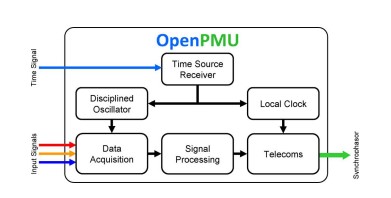
In order to lessen the restrictions of proprietary hardware and algorithms on the
progress of PMU development, the OpenPMU [10] group was formed, dedicated to designing ”open source platform for synchrophasor applications and research.” The group
utilizes a standard data acquisition device (DAQ) from National Instruments and a GPS
receiver from Garmin as the basis for the OpenPMU. A PIC from Microchip synchronizes
the DAQ to the GPS timecode. The OpenPMU uses the Python scripting language running on Microsoft Windows. It is currently able to measure synchrophasors, but has yet
to achieve full compliance with IEEE C37.118.1.
Design Requirements
3.1 Performance
A vast majority of the performance requirements for this project are drawn from the IEEE
Standard for Synchrophasor Measurements for Power Systems [11], its 2014 amendment
[12] and the IEEE Standard for Synchrophasor Data Transfer for Power Systems [13].
Two classes of performance are laid out in the standards: P, for fast response with no
explicit filtering and M, for analytic measurements sttausceptible to aliasing. Adherence
to these standards will ensure that the device is compatible with existing phasor data
concentrators (PDCs) and visualization software.
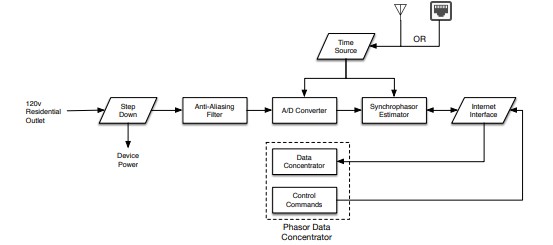
The device is broken down into seven different component parts as shown in Figure
3.1. The measurement source is a 120v residential outlet. A step down circuit lowers
the voltage of the measurement source into the range of the A/D converter. This circuit
will also provide DC power for the device itself. An analog anti-aliasing filter will be
used to limit the signal bandwidth before sampling. The signal passes through an A/D
converter that samples in synchronicity with the time source. The time source provides
an absolute time reference to the A/D converter and the Synchrophasor Estimator. The
Synchrophasor Estimator will calculate the magnitude of digital signal and run it through
a phase estimation algorithm (PEA). The resulting magnitude and phase estimation will
be given a time tag and sent to a PDC via the internet interface. The device must also
accept commands transmitted by the PDC.
3.1.1 Step Down and Device Power
Analog to Digital (A/D) converters are not typically capable of measuring signals at 120v,
meaning a voltage step down circuit must be designed to reduce the magnitude of the AC
signal to match the specified range of the A/D. The device may only have one connection to
the power source, meaning the step down circuit must also include a tap and rectification
circuit to provide power for the chosen processor. The supply circuit should have over
voltage protection to prevent damage to the device and have an output voltage ripple that
meets the constraints of the chosen processor.
3.1.2 Analog Filtering
Since an A/D conversion is being performed, it necessary to have an analog low-pass filter
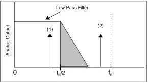
to reduce the bandwidth of the input signal and eliminate aliasing. The cutoff frequency for
the low-pass filter should be just above fs/2, the chosen sampling frequency. The desired
frequency response, defined in terms of the sampling frequency, is shown in Figure 3.2.

3.1.3 Timing
Synchrophasors must, by definition, be recorded with respect to an absolute time reference.
The absolute reference used by IEEE C37.118.1 is Coordinated Universal Time (UTC).
UTC can be obtained from either a GPS receiver or through the internet based Precision
Time Protocol (PTP) [15]. The time must be accurate within ±26µs according to the
standard. Receiving UTC via the internet is more practical for the scope of this project,
as GPS signals can be very weak indoors. However, testing is needed to confirm that
synchronization with internet time servers can be achieved with sufficient accuracy.
Each synchrophasor must be given a time tag according to Coordinated Universal
Time (UTC). The time tag consists of three numbers: a System On a Chip (SOC) count,
a fraction-of-second count, and a time status value. SOC is specified as a 4-byte binary
count of the number of seconds since the Unix epoch, 00:00 January 1, 1970. Occasionally,
a leap second must be inserted to keep SOC synchronized with UTC, which is specified
using a special case of the fraction-of-second as specified in section 4.3 of [11]. Time status
indicates the reliability of the clock, which can become unsynchronized due to loss of signal.
Values for time status are specified in Table 6 of [11].
3.1.4 Measurement
Synchrophasor measurements must be synchronized with the time code source so they can
be time-aligned with measurements from other PMUs by a PDC. Reporting rates are also
defined in IEEE C37.118.1 to ensure that multiple PMUs will take measurements at the
same rate.
Reporting Rate
The reporting rate, measured in phasors per second, must be a factor of the nominal system
frequency. Required rated are listed in Table 3.1. The reporting rate must be selectable
by the user via the device’s internet interface according to the protocol defined in [13].
Phase Estimation
There are two categories of phase estimation algorithms (PEAs): time domain and frequency domain. An example of a time domain PEA is the Weighted Least Squares method.
WLS uses a Taylor series expansion of the signal to determine the phase. In [16], variation
of the number of terms in the series is studied in an attempt to reduce error. The Interpolated Discrete Fourier Transform (IpDFT) is an example of a frequency domain algorithm. The IpDFT is significantly faster than WLS, but does not perform as well when disturbances occur. A thorough comparison between WLS and IpDFT is carried out in [16]. The selection of the PEA will provide the constraints for selection of a processor.
Total Vector Error
Total Vector Error (TVE) is a measurement of the difference between a perfect theoretical
phasor and the actual phasor measured by the PMU. The IEEE Std. C37.118.1 defines
TVE as:
T V E(n) = s
(Xˆ
r(n) − Xr(n))2 + (Xˆ
i(n) − Xi(n))2
Xr(n)
2 + Xi(n)
2
(3.1)
Where Xˆ
r(n) and Xˆ
i(n) are the real and imaginary components, respectively, of the measured phasor and Xr(n) and Xi(n) are the components of the theoretical phasor. The standard specified that TVE must be less than 1%. Sources of TVE include timing inaccuracy, off-nominal signal frequency, and low frequency oscillations.
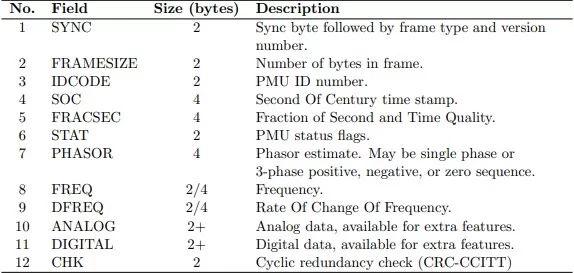
3.1.5 Communication
Communication between the PMU and PDC will take place via the internet. Data packets
will be sent using Transmission Control Protocol (TCP). Data packets are subdivided into
frames, each containing a specific piece of data. The frames required for sending phasor
data, as defined in IEEE C37.118.2, to a PDC are listed in Table 3.2. The phasor itself
is transmitted in frame 7. The DIGITAL frame can be used to transmit extra device
status indicators not included in the STAT frame, relay statuses, breaker statuses or other
information. The generic order of frame transmission is shown in Figure 3.3, where DATA1,
DATA2, etc. are frames 7-11 from Table 3.2
3.2 Safety
The device must comply with the National Electric Code regulations for connection spacing and insulation for 120v connections [17]. The connection to the wall outlet should be made with a NEMA 5-15 compliant connector as it is the most common outlet found in residences. The connector is rated for a maximum voltage of 125v, sufficient for the requirements of this project.
3.3 Cost
Commercial PMUs cost an average of $43,400 per installation [3]. This device will be installed en masse in residences and should have a cost commensurate with mass production. The target cost for this project is under $1,000.
Design Alternatives
4.1 Component Selection
4.1.1 Computing Platform
The computing platform is the core of the phasor measurement unit. It is responsible for
acquiring raw AC voltage waveform data from an Analog to Digital Converter (ADC) in
synchronicity with the GPS Pulse Per Second (PPS) time code, computing the magnitude
and phase of the signal, packaging the measured data into the IEEE C37.118.2 transmission
format and sending the resulting data packet over the internet to a PDC. Many options
were considered in the choice of the computing platform for this project, including the wellknown Raspberry PI, the Arduino, BeagleBone Black, and Intel Edison. The Raspberry PI, while it is a relatively powerful platform with thorough documentation and an active
user base, was dismissed due to the lack of an onboard ADC. Choosing a platform with
an onboard ADC is important because it simplifies the circuitry and reduces the cost of
the device. An Arduino, while it has an onboard ADC, lacks the computing power of the
other SOC based alternatives, requires additional components to connect to the internet, and does not have the ability to be reprogrammed remotely, an important consideration when deploying a device in the homes of laymen residents. Intel’s Edison platform was considered for its high computing power density (dual core 500 MHz processor), but rejected due to the scarcity of public documentation. Ultimately, the BeagleBone Black was chosen as the computing platform. It has a 1 GHz processor, which outperforms the Raspberry PI’s 700 MHz, a built in ethernet port for internet connection, and an onboard ADC with eight input channels. The Black also can run the Debian or Ubuntu Linux distributions. Using these Linux distributions provides built in for remotely accessing the device and a large package database to pull from when implementing components of the project. Of the most consequence in choosing this board was the NEON and Programmable Realtime Unit (PRU) subsystems. The NEON subsystem provides hardware acceleration for floating point calculations and a implementation of the Fast Fourier Transform that utilizes this capability has already been developed. Utilizing this library will allow for the reduction of the computational load on the processor, which in turn should enable the device to achieve a higher reporting rate. The PRU, essentially an onboard microcontroller in which the execution of each instruction is fixe is significant because all of the instructions available in this subsystem have a fixed execution time of 5ns. The PRU interfaces directly with the ADC subsystem and the Black’s onboard memory, meaning it can acquire data from both the GPS and AC voltage inputs to the ADC and store it for processing in a fixed, known amount of time that can be easily compensated for in the final calibration of the device.
4.1.2 GPS Module
As stated in the Timing section of the Design Requirements, the time source must be
accurate within ±26µs in order to achieve the accuracy specified in [11]. There are many
timing-specific GPS modules on the market, but their average price is $450, [18] which is
prohibitive for the budget of this project. The Adafruit Ultimate GPS Module is offered at
a reasonable $40 and achieves ±9µs accuracy [19] on its PPS output. Though this is not
as accurate as timing-specific sources, some boast sub ±5µs accuracy, [20] it is well within
the specifications and budget for this device.
4.2 Software Design
4.2.1 Signal Processing
From the initial stages of the project, Python was the desired programming language for
processing raw data into synchrophasor measurements. Availability of Python packages for
signal processing and ethernet packet transmission, cross platform compatibility, and the
ease with which the language can be interpreted by a lay person were the driving factors in
this choice. By choosing such a widely known and supported language the code generated
in this project can be of greater utility to others researching PMUs. However, Python
is a high-level programming language which presents a few challenges when interacting
directly with hardware. Python code has to be parsed by the Python interpreter before it
is executed, exacting a performance penalty. In addition, low-level programming languages
like C are more suited to direct memory interaction than Python.
It was possible to use Python, despite its deficiencies, in this project because the heavy
lifting is handled by the PRU. Samples generated by the ADC are stored in shared memory
accessible from the CPU by the PRU, which ensures that latency between sample acquisition and storage in memory is a fixed, known value. Texas Instruments, the designer
of the AM335x processor onboard the BeagleBone Black, provides a library for sending
assembly code to and monitoring interrupts from the PRU written in C, another obstacle.
Fortunately, PyPRUSS, a community project focused on 3D printing with the Black [21],
incorporates a Python wrapper for the C library, enabling its functions to be called within
Python code.
4.2.2 Signal Acquisition
Acquisition of data with the BeagleBone Black’s onboard ADC can either be handled by the
CPU or by the PRU. The host CPU runs Debian, a variant of linux, which is not a realtime
operating system. Any processes interacting with the ADC are scheduled at the mercy of
the operating system, which is not a desirable characteristic in an application where precise
timing is of the utmost importance. Therefore, the PRU was used to communicate with the
ADC subsystem. The PRU is controlled with assembly code loaded by the CPU. Coding
in assembly presents a few challenges; operations involve direct manipulation of registers
and memory locations which is time consuming and potentially catastrophic as the PRU
has access to the memory and storage used by the operating system. Ultimately, the tight
timing constraints imposed by the design requirements necessitate the use of the PRU
despite the faults of coding in assembly.
Preliminary Proposed Design
5.1 Hardware Design
5.1.1 Voltage Step Down
Connection to the wall will be made with a NEMA 5-15 compliant connector, the common standard for residential outlets [17]. The ADC input range of the BeagleBone Black is 0 to 1.8v [22], but going directly to this range would require a transformer ratio of 66.7:1 or greater, something that is not commonly found in 120v transformer offerings. A 14:1 transformer was chosen instead because of its availability and price. This transformer yields a 8.57v peak-to-peak output when connected to the 120v wall outlet. The voltage
is further reduced into the ADC range by attenuation in the low pass filtering circuit.
Input Protection
Although 120v is not as dangerous as the high voltage that commercial PMUs measure, it is important that this device have safety features to protect both the low voltage electronics and the end user. A 0.5A fast-acting fuse was placed between the hot wire of the plug and the device as the power supply for chosen for the BeagleBone Black has a maximum current draw of 0.3A. The digital (DGND), analog (GND ADC), and earth grounds as well as the neutral wire are all tied together to ensure that there are no ground loops that might affect measurement, but also to ensure that any shorts or loose wires will not generate unexpected voltages throughout the circuit.
DC Bias
It is also necessary to add a DC bias to the AC signal in order to fall within the 0 to 1.8v range. This is accomplished by a simple DC bias circuit shown in Figure 5.1. The resistor connected from the input terminal to ground is important because it ensures that the input is at 0v before a connection is made, protecting the measurement source from any
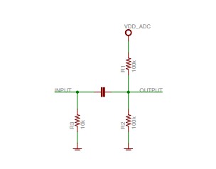
unexpected charge on the capacitor. The DC bias voltage will be generated by a voltage divider between VDD ADC and ADC GND with equal value resistors to ensure the mean of AC signal falls exactly in the middle of the input range.
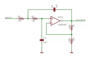
5.1.2 Anti-Aliasing Filter
PMUs typically sample at relatively low rates, 3kHz or less, as the nominal frequency of the power grid is only 60Hz. It is essential to low pass filter the signal before it is sampled as sampling at such a low rate means there is a much higher chance of aliasing. As gain reduction is desired, a non-inverting active low-pass filter was chosen. The BeagleBone Black is a single supply board necessitating a single supply operational amplifier be used in the filter, specifically the LM358 which both met the specifications and was already available in the lab. A DC coupled low-pass RC active filter design presented in the LM358 datasheet [23] was used as the basis for the design of this circuit. Resistor and capacitor values, listed in the circuit schematic in Figure 5.2 were calculated using the equations provided in the datasheet with a cutoff frequency of 100Hz, gain of 0.2 and quality factor of 1 as the design parameters. Filters inherently generate a phase difference between the
input and output signals; it is important that this phase shift is measured and accounted for in the final calibration of the device.
5.1.3 Analog to Digital Conversion
Sampling is handled by the touchscreen controller and analog-to-digital converter subsystem (TS ADC SS). The systems was designed to be used as a digitizer for touch screen input, but can also operate as a regular ADC when set to general purpose mode. Analog input can range from 0 to 1.8v and there are 8 channels available on the BeagleBone Black. However, the 8 channel count is somewhat misleading as there is only one ADC. Channels
are multiplexed to the ADC, as shown in Figure 5.3, meaning that channel capture can only happen sequentially. Multiplexing of channels is controlled by a finite state machine with sixteen sequence steps. Each step corresponds to the acquisition and storage of data from one channel as outlined in Figure ??. Two steps will be used to acquire both the AC voltage waveform and the pulse per second signal from the GPS. The minimum delay between sampling steps is 15 ADC clock cycles, a value that must be taken into account
in the calibration of the device.
5.1.4 GPS Timing
The Ultimate GPS module from Adafruit is largely self-contained, necessitating only a few external connections to enable functionality of the chip. An onboard voltage regulator enables the use of sources from 3.3 to 5v, both of which are available on the pinout of the BeagleBone Black. 3.3v was chosen for the supply voltage simply because the 5v pin was already connected to the low pass-filter circuit. Communication between the GPS module and the Black is handled by the Universal Asynchronous Receiver Transmitter (UART).National Marine Electronics Association (NMEA) sentences, a standard format for GPS data, are received from the GPS via UART and used to assign UTC time tags to phase measurements.
The PPS signal is acquired via the onboard ADC in conjunction with the AC voltage waveform. This signal serves as the marker for the start of a Discrete Fourier Transform (DFT) window. The output of VFix, which is pulled low when a strong signal is found, is connected to a general purpose input output, indicating when the GPS is ready for measurement to begin.
5.2 Signal Processing
5.2.1 Sampling Rate
The sampling rate of ADC acquisitions is controlled both by dividing the ADC clock and by increasing the delay between measurement steps. Both methods will be implemented to achieve sampling at an integer multiple of 60Hz, desired to ease the processing requirements once sampled.
5.2.2 Raw Data Processing
Data from the ADC is stored as a 32 bit hex value. Both the four bit channel ID and the twelve bit converted value are contained within these 32 bits. Two bitwise shift operations are used to extract each component and then the values are converted to integers for further processing.
Source: Design of an Inexpensive Residential Phasor Measurement Unit