
From smart TVs with gesture control to the high-resolution cameras integrated into today's smartphones to applications boasting multiple cameras, image processing has become a key component in many consumer electronics products. To support the need for more pixels and fast-changing requirements, designers are finding that they must offload some image processing from the application processors. That's why image system processing (ISP) is integral to the design of today's systems on chip (SoCs).
Processing devices that can perform camera control and even inline processing for applications such as gesture control can enhance a simple application processor camera receiver interface. However, designing SoCs with image processing capabilities can be a time- and labor-consuming process, typically calling for six to nine months of commitment. Given the time-to-market pressures of designing for the consumer market, not to mention the different image processing requirements for different applications, this is a time commitment that most designers would probably prefer to shorten.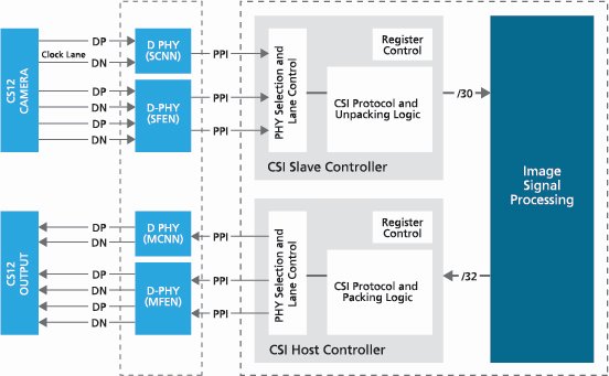
Cadence offers MIPI® intellectual property (IP) which is used in an ISP development platform that can reduce the development time of image processing algorithms integrated into SoCs. MIPI interfaces for camera applications are expanding rapidly into inline video image processing. With this type of development, it's useful to have a flexible platform on which to develop the processing algorithms. It’s even more advantageous to implement these algorithms in an FPGA for a performance evaluation–before the silicon design is sent to the fab.
Co-Development Platform for ISP
The Cadence® ISP development sub-system consists of configurable and pre-verified MIPI IP blocks–the CSI-2 receiver controller (slave), the CSI-2 transmitter controller (master), and MIPI D-PHY core. All of the IP cores have been verified with the Cadence Verification IP (VIP) Catalog. This integrated system runs on an FPGA platform with a D-PHY test chip and can support multiple camera vendors with a simple adaptor board.
Cadence MIPI controllers are designed to fit seamlessly into image subsystems and can be provided as a truly integrated solution with the Cadence D-PHY, simplifying the integration process for the user.
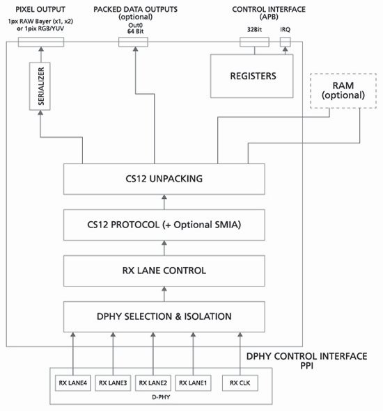
Cadence's CSI-2 RX slave controller is a camera serial interface IP that supports:
- MIPI CSI-2 protocol-based data received on MIPI D-PHY PHY protocol interface (PPI)
- Virtual channel/data type interleaving
- Protocol error detection/correction including error correcting code (ECC) and cyclic redundancy check (CRC)
- D-PHY and lane swapping of up to four 1.5Gbps data lanes
- Pixel output and/or 64-bit packed outputs (configurable)
- SMIA-based 64-bit packed Interswitch Link (ISL) (configurable)
- All primary and secondary data formats including RGB/YUV and RAW as specified in Table 8 Primary and Secondary Data Formats Definitions, MIPI Alliance Specification for Camera Serial Interface 2 (CSI-2) version 1.1
- MIPI D-PHY PPI, MIPI Alliance Specification for D-PHY version 1.7, Appendix A
Cadence's CSI-2 TX master controller is a camera serial interface IP that supports:
- Virtual channel/data type interleaving
- Protocol error detection including ECC and CRC
- D-PHY and lane swapping of up to four 1.5Gbps data lanes
- Continuous and gated clock configurations
- All primary and secondary data formats including RGB/YUV and RAW as specified in Table 8 Primary and Secondary Data Formats Definitions, MIPI Alliance Specification for Camera Serial Interface 2 (CSI-2) version 1.1
- MIPI D-PHY PPI, MIPI Alliance Specification for D-PHY version 1.7, Appendix A
- Cadence's MIPI D-PHY is PHY IP that supports:
- High-speed and escape TX or RX clock lane and up to four data lanes
- High-speed differential inputs (RX) and outputs (TX)
- MIPI defined PPI
 Optimizing ISP Before Silicon
Here's the flow of data in the ISP development system: a camera source sends CSI-2 data to the D-PHY test chip card and connects to an FPGA development board. Since this involves relatively low speed requirements, the PPI from the D-PHY test chip is passed into the FPGA via standard I/Os. The PPI also connects to the CSI-2 RX slave controller. The slave controller passes out unpacked pixel data and associated synchronization information to the ISP block that contains the ISP algorithm under test. The ISP passes out pixel data to the CSI-2 TX host controller, which applies the CSI-2 protocol to packetize the data to be sent across the PPI to a second D-PHY test chip card. The serial data from the D-PHY test chip card connects via SMA connectors to a SMA-to-CSI-2 flexi cable connector. This flexi cable connects to a Raspberry Pi (low-cost computer) CSI-2 port. The data received into the Raspberry Pi board can then be sent out to a display through the Raspberry Pi's HDMI port.
This setup provides a platform for an engineer to develop and then optimize a software-based image processing algorithm that can then be ported to the FPGA using a C-to-register-transfer level (RTL) system. (Cadence C-to-Silicon Compiler, for example, is a high-level synthesis tool that generates implementation-ready RTL for a target application.) Before any commitment to silicon, algorithms can be compiled into the FPGA and optimized while maintaining the video output using Raspberry Pi video display support.
For more detail: Fast Development of ISP Algorithms with MIPI IP and FPGA Platform