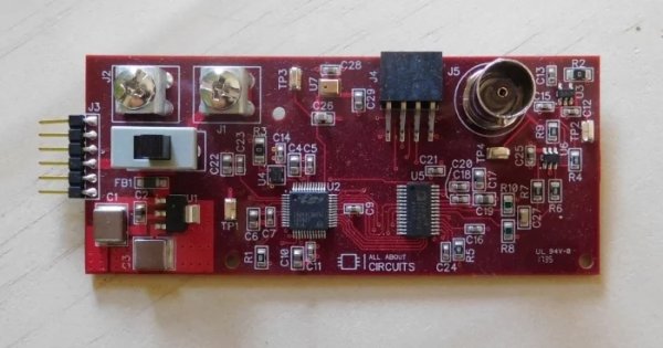
I recently designed an arbitrary waveform generator (AWG) PCB that is built around a C8051F360microcontroller and a TxDAC from Analog Devices.
These two ICs communicate via a parallel interface that allows me to generate higher-frequency analog signals by seeking the maximum rate at which the microcontroller can move data to the DAC.
In this article I won’t go out of my way to explain aspects of the hardware design, because I have extensively discussed the schematic and layout in a series of preparatory technical articles. Three of these articles focus on a particular portion of the schematic (namely, the microcontroller, the DAC, and the DAC’s output circuitry), and the fourth one covers the layout. For PCB development visit FS PCBA
The Objective
The goal of this project is to create the firmware framework that will allow us to conveniently move digital data from the microcontroller to the DAC, and then convert this data into an analog signal. This AWG board has the potential for some interesting functionality, but the most important step is to establish a reliable, extensible, high-precision interface between the MCU and the DAC. We’ll verify this interface by generating a ramp waveform and by performing some oscilloscope analysis.
The Requirements
High-Precision Timing
Many microcontroller applications have little if any need for highly accurate timing. This is why we can so often create successful devices in which the only clock source is the MCU’s low-precision internal oscillator. But the AWG is different. We want to generate signals that are as consistent as possible with the idealized mathematical waveforms that serve as the source material, and this means that we need predictable signal frequencies and a consistent DAC sampling rate.
Efficient Use of the Processor
Though this particular PCB is almost completely devoted to generating waveforms, we need to ensure that this firmware-plus-hardware framework can be readily incorporated into other applications. Consequently, we want our firmware to be able to generate stable, high-precision waveforms but without rendering the processor completely unavailable for other tasks.
Maximum Speed
We live in a high-frequency world, and this AWG will be of little use if it maxes out at 1 kHz. In all fairness, this is a straightforward, low-cost design, and we can’t expect it to create 915 MHz DQPSK waveforms ready for ISM-band transmission. But we want to get as much bandwidth out of this device as we can, and this is all the more challenging when we remember that the sampling frequency is significantly higher than the actual signal frequency. The Nyquist–Shannon theorem notwithstanding, I want at least five samples per cycle, and ten is my preference. So even if we manage to push the sampling rate up to 10 MHz, our waveforms will be down in the 1–2 MHz range.
The hardware design already reflects the importance of optimizing for speed: I chose a microcontroller that operates at core frequencies up to 100 MHz, and I implemented a parallel bus that minimizes the overhead required to move data from the MCU’s memory to the DAC input pins.
Sampling Rate
The AWG board has a high-performance clock source (a MEMS oscillator with overall frequency stability of ±50 ppm). The firmware needs to use this time base to create a stable clock signal that drives the DAC’s update circuitry. When I want high-quality timing signals I always turn to hardware, and in this case I’m using the programmable counter array (PCA) to generate a 500 kHz clock from the 10 MHz external oscillator.
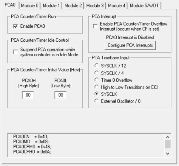
I used the Silicon Labs Config2 program for my hardware configuration, because the C8051F360 is not supported by the configuration tool that is incorporated into Simplicity Studio. Here is the general configuration for the PCA module:
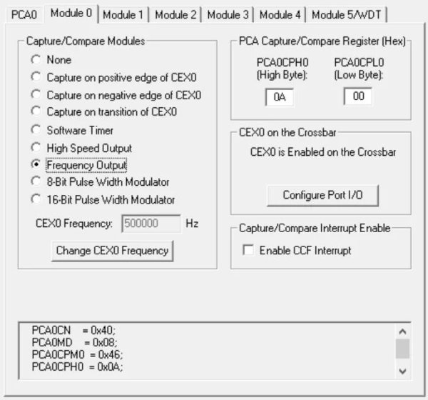
The PCA is enabled and the time base is the system clock. At this point the system clock frequency is the same as the external oscillator frequency (10 MHz), but later we’ll use the microcontroller’s phase-locked loop to obtain a higher core frequency. The DAC’s clock signal is generated by PCA module 0 configured for “frequency output” mode:
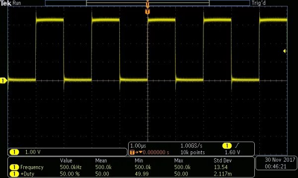
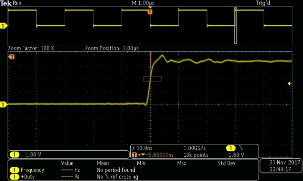
Let’s take a look at the sample-rate clock. My MDO3104 scope from Tektronix has some fairly advanced measurement capabilities that will help us to assess its quality.
As confirmed by the measurements displayed at the bottom of the scope capture, the frequency is exactly as expected (500 kHz), and we also have a perfect 50% duty cycle; furthermore, the “Min” and “Max” statistics indicate that the frequency and duty cycle are stable over time.
A particularly helpful addition to this measurement functionality is the standard deviation (“Std Dev”). Standard deviation indicates how much the values tend to deviate from the mean, and in this situation it’s a quick and easy way to assess imperfections in the frequency and duty cycle of the clock signal. Both of the standard deviations are very low: 13.54 Hz is 0.0027% of the nominal frequency, and 2.117×10⁻³ is only 0.0042% of the typical duty cycle.
We can take this analysis a step further by looking at the histogram of one of the clock edges. If we set the scope to trigger on the falling edge and then zoom in on the rising edge, the position of the rising edge will shift according to the signal’s jitter. We can then add a horizontal waveform histogram to track this jitter and reveal its distribution. In this case, though, there isn’t much to see, because the jitter is so low.
The External Interrupt
We now have a square wave that controls the DAC’s output circuitry; the next task is to synchronize the MCU’s data updates with this square wave. We will do this by attaching an external interrupt to the PCA pin that outputs the clock signal. The DAC latches the input data on the rising edge of the clock, so we want to update the data signals on the falling edge. This opposite-edge technique is the fundamental way to ensure that digital data is updated and stabilized before the input device receives the active clock edge.
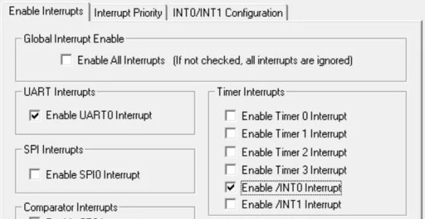
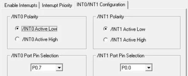
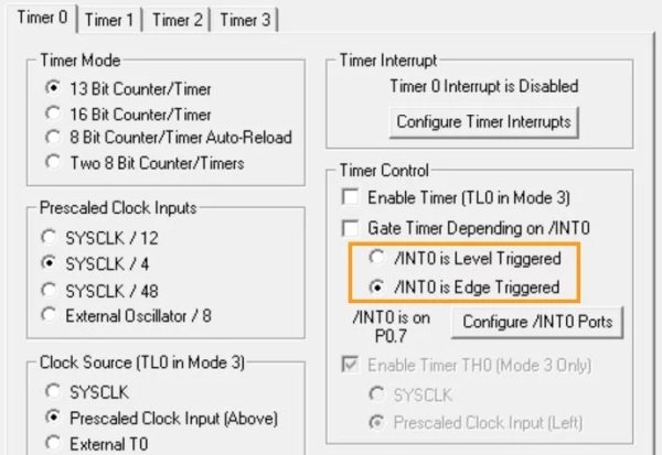
So, I enabled external interrupt 0 (denoted /INT0), attached it to the clock-signal output pin (P0.7), and made it sensitive to the falling edge.
You are probably accustomed to using an external interrupt to monitor an input signal, but in this case it can just as effectively synchronize firmware events with a signal generated by the microcontroller itself. This is actually a particularly handy strategy when you’re dealing with a timing-critical task, because external interrupt 0 is the highest-priority interrupt, and because its interrupt-pending flag is automatically cleared by hardware (which eliminates whatever time would be required to clear the flag using a firmware statement).
The ISR
The main action takes place in the /INT0 interrupt service routine. The next DAC data byte is retrieved from memory (or generated directly by the microcontroller) and then driven onto P2; I used a #define statement to make “DAC_WORD” an alternative to “P2”:
SI_INTERRUPT(INT0_ISR, INT0_IRQn)
{
DAC_WORD–;
}
The critical variable in the effort to maximize the DAC update rate is the amount of time required to execute the instructions in the ISR. (In this example we have only one instruction, but that won’t always be the case.) The ISR must be called once for every active edge of the DAC clock, and we can’t call the ISR before it is done executing. So when we try to push our bandwidth to the maximum, we will need to do whatever we can to minimize the ISR’s execution time, and then we will set our DAC-clock frequency accordingly.
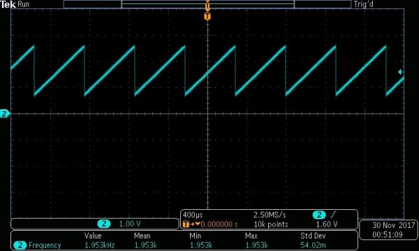
The single statement shown above (DAC_WORD–) creates a ramp waveform, because the DAC value decreases linearly to zero and then rolls over to 255 and starts decreasing again. Here is the output from the DAC:
You may have noticed that the analog ramp sections increase toward the maximum voltage, whereas the DAC values decrease toward zero. This occurs because the DAC’s output amplifier uses an inverting configuration.
Let’s look at one last scope capture before we finish up.
Read More Information….
How to Generate a High-Precision Waveform Using a DAC and a Custom PCB


