
Heightened accuracy and speed in an operational amplifier (op amp) has a direct relationship with the magnitude of its power consumption. Decreasing the current consumption decreases the gain bandwidth; conversely, decreasing the offset voltage increases the current consumption.
Many such interactions between op amp electrical characteristics influence one another. With the increasing need for low power consumption in applications like wireless sensing nodes, the Internet of Things (IoT) and building automation, understanding these trade-offs has become vital to ensure optimal end-equipment performance with the lowest possible power consumption. In the first installment of this two-part blog post series, I’ll describe some of the power-to-performance trade-offs of DC gain in precision nanopower op amps.
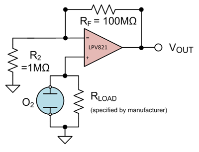
DC gain
You probably remember from school the classic inverting (Figure 1) and noninverting (Figure 2) gain configurations of op amps.
These configurations resulted in inverting and noninverting op amp closed-loop gain equations, Equations 1 and 2, respectively:
where ACL is the closed-loop gain, RF is the value of the feedback resistor and R2 is the value of the resistor from the negative input terminal to signal (inverting) or ground (noninverting).
These equations are a reminder that DC gain is based on resistor ratio, not resistor value. Additionally, the “power” law and Ohm’s law show the relationships between resistor value and power dissipation (Equation 3):
where P is the power consumed by the resistor, V is the voltage drop across the resistor and I is the current through the resistor.
For nanopower gain and voltage divider configurations, Equation 3 tells you that, in order to minimize power dissipation, you need to minimize the current consumption by the resistor. Equation 4 helps you understand the mechanism to do that:
where R is the resistor value.
Using these equations, you can see that you must choose large resistor values that provide both the gain you need while minimizing power dissipation (and therefore power consumption). If you don’t minimize current through the feedback path, you’ll lose the benefit of using nanopower op amps.
Once you’ve determined what resistor values will meet your gain and power-consumption needs, you’ll need to consider some of the other op amp electrical characteristics that will affect the accuracy of signal conditioning. Summing several small systemic errors inherent in nonideal op amps will give you the total offset voltage. The electrical characteristic, VOS, is defined as a finite offset-voltage number between the op amp inputs, and describes these errors at a defined bias point. Please note that it does not describe these errors across all operating conditions. To do that, you must consider the gain error, bias current, voltage noise, common-mode rejection ratio (CMRR), power-supply rejection ratio (PSRR) and drift. Covering all of these parameters is beyond the scope of this post, but let’s look at VOS and drift – and their influence in nanopower applications – in a bit more detail.
Read more: How to make precision measurements on a nanopower budget