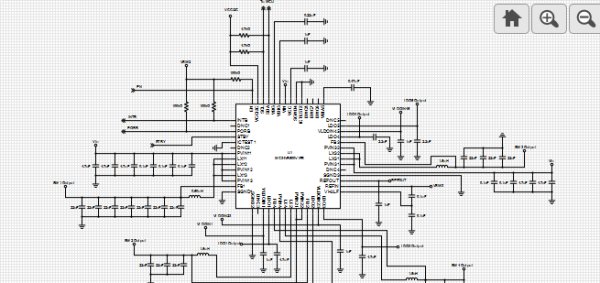
The circuit in this reference design features the capability of MC34VR500V1ES to supply multiple DC voltage outputs. This device is designed to support the LS1/T1 family of communication processors, which require efficient and precise level of voltage supplies. With its four switching and five linear regulators, the MC34VR500V1ES can supply power to the whole system, e.g., the processor, memory, system peripherals.
The MC34VR500V1ES device runs with a supply voltage ranging from 2.8V to 4.5V. It can provide nine outputs. Four of these outputs (SW1-4) are buck regulators while the rest (LDO1-5) are general purpose LDOs. Each one of the buck regulator is capable of operating in Pulse Frequency Modulation (PFM), Auto Pulse Skip (APS), and Pulse Width Modulation (PWM) switching modes. These buck regulators also have a current limit feature that generates a fault interrupt whenever there is an overcurrent condition. The SW1 output is capable of providing 0.625-1.875V/4.5A supply while SW2 and SW3 can provide 0.625-1.975V/2A and 0.625-1.975V/2.5A, respectively. The SW1, SW2 and SW3 voltages can be varied with a step size of 25mV. The SW4 output is half of the voltage output of SW3. The general output LDOs can output voltages ranging from 1.8-3.3V with a step size of 100mV except for LDO1 which can only give 0.8-1.55V output with 50mV step size. The LDO1 output can provide current up to 250mA, while LDO2 and LDO4 can output up to 100mA only. The LDO5 output can provide 200mA of current while LDO3 can output up to 350mA. Aside from these nine outputs, the MC34VR500V1ES also have a REFOUT output dedicated for DDR memory reference voltage. The voltage of this REFOUT output is usually half of the SW3 output and can only provide up to 10mA of current. The MC34VR500V1ES outputs can be changed by programming it via the I2C interface.
The operation of the MC34VR500V1ES can be reduced to four states, or modes: ON, OFF, Sleep, and Standby. For the device to turn ON, the input voltage must surpass a voltage threshold of 3.1V, the EN pin must be high, and PORB is de-asserted. The 34VR500 enters the OFF mode when the EN pin is low or there is a thermal shutdown event that forces the device into the OFF mode. Standby mode is usually entered when the STBY pin is asserted for low-power mode of operation. The device only goes into sleep mode if the EN pin is de-asserted. To exit sleep mode, assert the EN pin.
For more detail: MC34VR500V1ES Multi-Output DC/DC Regulator


