The Xilinx Artix dev kits that fit in your laptop. A convenient, affordable way to explore Xilinx PCIe IP.
PicoEVB is an affordable, open source, development board which can be used to evaluate and prototype PCI Express designs using a Xilinx Artix 7 FPGA on Windows or Linux hosts. The boards are designed around the Artix 7 (XC7A50T).
Use Cases
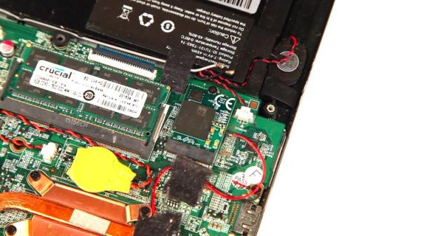
While the main intent of PicoEVB is PCIe design prototyping, it can be used as an integrated part of your laptop (or desktop) computer. Use a board as an encryption co-processor for security, or as a hardware-level encoder/decoder for speedy workflows. It’s your FPGA, design what you like.
Features & Specifications
| Feature | PicoEVB |
|---|---|
| FPGA | Xilinx Artix XC7A50T |
| Form Factor | M.2 (NGFF) 2230, keyed for A and E slots |
| Dimensions | 22 x 30 x 3.8 mm |
| Host Interface | PCIe x1 gen 2 |
| Host Tools | Vivado 2016, 2017 |
| MGT Loopback | Yes |
| Built-in JTAG | Yes |
| External Interface | 4 digital channels OR 1 analog (differential) and 2 digital, OR 2 analog (differential) |
| User-controllable LEDs | 3 |
Open Source Software & Hardware
The board schematics in their final form (PDFs) will be published under a permissive license. In additon, major software components are open source:
- The “cable driver”, is already CC0 licenced.
- All of the host code (PCIe drivers) used in the prototype comes from Xilinx under GPL.
- The FPGA project is derived from a freely available Xilinx sample project.
Files are being published in the project GitHub repository.
PicoEVB Block Diagram
Compact Size
Current FPGA development boards are large. Almost all development kits require a desktop PC, or are designed to sit on a lab bench. NanoEVB aims to change this – the entire development kit fits inside a laptop! In addition, the JTAG cable is built-in, no external cables needed- just plug it into a PCIe slot and go.
Affordable
Furthermore, to explore PCIe designs, currently you need to spend over $1,000. NanoEVB and PicoEVB have PCIe connectivity to the host computer, and as such, you can design PCIe-based solutions and explore Xilinx’s IP for PCIe solutions without spending a grand and without taking up a ton of space.
Manufacturing Plan
The manufacturing process for NanoEVB and PicoEVB is pretty straightforward:
- Select a PCB fabrication house capable of producing this PCB (done)
- Select an assembly house capable of placing/soldering all the parts on the PCB (quote in-hand, with more to come)
- Kit the PCBs and board components and ship to assembly house for assembly
- Final test of assembled boards to verify all power supply voltages, all LEDs, all external ports, and USB and PCIe connectivity.
Read more: NanoEVB & PicoEVB – Xilinx Artix Developemtn kits


