
STMicroelectronics has revealed a new family of GaN power semiconductors in the STPOWER portfolio that can significantly reduce energy use and enable slimmer designs in a huge variety of electronic products
Target applications include consumer equipment such as chargers, external power adapters for PCs, LED-lighting drivers, and power supplies inside televisions and home appliances. Produced in high volumes and, with greater efficiency, this equipment can deliver significant CO2 savings. In higher-power applications, ST’s PowerGaN devices are suitable for telecom power supplies, industrial motor drives, solar inverters, and electric vehicles and chargers.
“Commercialising GaN-based products is the next frontier for power semiconductors, and we are ready to realise the potential of this exciting technology. ST is announcing the first product in a new family, belonging to the STPOWER portfolio, that can deliver breakthrough performance for a large variety of power supplies across consumer, industrial, and automotive applications,” said Edoardo Merli, Power Transistor Macro-Division General Manager and Group Vice President of STMicroelectronics’ Automotive and Discrete Group. “We are committed to progressively building up our PowerGaN portfolio to enable customers to design more efficient, smaller power supplies everywhere.”
Gallium Nitride (GaN) is a compound wide-bandgap semiconductor material capable of supporting far higher voltages than traditional silicon without compromising on-resistance thus reducing conduction losses. Products implemented in this technology can also be switched much more efficiently, resulting in very low switching losses. The possibility of operating at higher frequencies implies the adoption of smaller passive components.
All these features will enable designers to cut total losses (reduce heat generated) and improve efficiency in power converters. As a result, GaN allows for miniaturisation, making a PC adaptor smaller and lighter than today’s ubiquitous chargers, for example.
According to a third-party estimate, a standard mobile phone charger can be reduced by up to 40% in size when using GaN components, or it can be designed to deliver more power in the same size. Similar performance improvement in efficiency and power density can be envisioned for a broad number of applications across consumer, industrial, and automotive electronics.
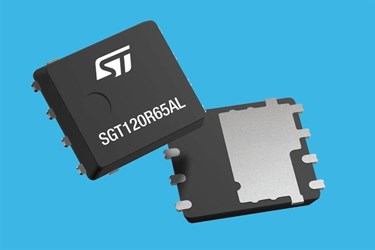
The first device in ST’s new G-HEMT transistor family is the 650V SGT120R65AL with 120mΩ maximum on-resistance (RDS(on)), 15A maximum current capability, and a Kelvin source connection for optimum gate driving. It is available now in an industry-standard PowerFLAT 5×6 HV compact surface-mount package – typical applications are PC adaptors, USB wall chargers, and wireless charging.
650V GaN transistors in development are available now as engineering samples. These include the SGT120R65A2S with 120mΩ RDS(on) in an advanced laminated package, the 2SPAK™, which eliminates wire bonding to boost efficiency and reliability in high-power and high-frequency applications, as well as the SGT65R65AL and SGT65R65A2S both with 65mΩ RDS(on) in PowerFLAT 5×6 HV and 2SPAK, respectively.
Volume production for these products is expected in H2 2022.
In addition, a new cascode GaN transistor, the SGT250R65ALCS with 250mΩ RDS(on) in a PQFN 5×6, belonging to the G-FET family, will be available for sampling in Q3 2022.
The G-FET transistor family is a very fast, ultra-low Qrr, robust GaN cascode or d-mode FET with standard silicon gate-drive for a wide range of power applications.
G-HEMT transistor family is an ultra-fast, zero Qrr e-mode HEMT, easily parallelable, well suited for very high frequency and power applications.
Source: STMicroelectronics introduces first PowerGaN products