
Such is the popularity of DC-to-DC voltage converters (“switching regulators”)––due to their high efficiency across wide input- and output-voltage ranges––that chip makers have focused a lot of research dollars on squeezing the essential components of the devices into modules. These modules typically include pulse-width-modulation (PWM) controllers and switching elements in a single, compact package, easing the design work for the engineer.
However, until recently, it has proven difficult to include the energy-storage device (the inductor) inside the package. This has dictated that the engineer must specify, source, and design-in the inductor as a peripheral component, adding complexity and consuming board space. Now, a new generation of high-frequency switching regulators has enabled the use of smaller inductors enabling the devices to be housed inside the component vendor’s package.
This article briefly explains the role of an inductor in a switching-regulator design before moving on to describe the technical merits and trade-offs of selecting a power module with an integrated inductor.
Anatomy of a switching regulator
Switching regulators use a switching element (typically one or two metal-oxide semiconductor field-effect transistors (MOSFETs)) and an energy-storage device (an inductor) to efficiently regulate an input voltage to a lower (“buck”) or higher (“boost”) output voltage.
The inductor performs a fundamental role in the switching regulator. In a buck regulator, when the transistor is powered, the magnetic field in the inductor builds up, storing energy. The voltage drop across the inductor (which is proportional to the duty cycle of the transistor) opposes (or “bucks”) part of the input voltage. When the transistor switches off, the inductor opposes the change by flipping its electromotive force (EMF) and supplies current to the load itself via the diode.
In a boost converter current flows from the input when the transistor is switched on. This passes through the inductor and transistor, with energy being stored in the inductor’s magnetic field. There is no current through the diode, and the load current is supplied by the charge in the capacitor. Then, when the transistor is turned off, the inductor opposes any drop in current by reversing its EMF, boosting the source voltage, Current, due to this boosted voltage, flows from the source through the inductor and diode to the load, as well as recharging the capacitor (Figure 1).
In a buck converter under steady-state conditions, the average current in the inductor (IL) is equal to the output current IOUT. Due to the voltage input being a square wave, the inductor current is not constant, but ripples between a maximum and a minimum value as the input voltage switches on and off. The difference between the maximum and minimum (ΔIL) is called the peak-to-peak inductor-current ripple (Figure 2).
In turn, the current ripple, combined with the output filter capacitor’s equivalent series resistance (ESR), causes the output voltage to ripple around the set voltage (see the TechZone article “Capacitor Selection is Key to Good Voltage Regulator Design”).
The choice of inductor is determined in part by the desired peak-to-peak value of the inductor current and the switching frequency. For a given operating frequency, a larger inductor reduces the peak-to-peak current (because the current ramp-up and -down is shallower for such a winding). However, the Inductor value is inversely proportional to switching frequency for equal peak-to-peak ripple current. By increasing the switching regulator’s operating frequency, an inductor with fewer loops and/or thinner wire for the coil, and a smaller core can be used, reducing the inductor’s volume due to the fact that by operating at a high frequency the inductor does not have to store as much energy between switching events[1] (also see the TechZone article “The Inductor’s Role in Completing a Power Module-Based Solution”).
Tiny inductors inside
Major semiconductor vendors supply a wider range of power modules that incorporate most of the components of a switching regulator into a convenient compact package. Typically these modules integrate the PWM controller and switching element(s) into a silicon device leaving the designer with the job of selecting passive components for the input and output filters to match their application. However, these chips do not incorporate the inductor because, as yet, it has proved impossible to shrink the coil such that it becomes a silicon feature.
For example, Intersil’s ISL85415 buck-switching regulator integrates two MOSFETs and a PWM controller onto a single chip but requires an external inductor. This power module operates from an input voltage range of 3-36 V and supplies 0.6-34 V at up to 500 mA. The switching frequency can be adjusted in the range 300 kHz to 2 MHz.
The exclusion of the inductor from a power module leaves the designer with the challenge of specifying a suitable device for his or her power supply. (For example, the Intersil device described above employs a 22 µH external inductor in a typical application circuit.) While there is a wealth of vendor applications notes advising how to go about the process and a wide range of suitable inductors, this is not a trivial task. For example, it can be all too easy to specify a device that appears perfect for the job but in practice causes the switching regulator to drop into a discontinuous operating mode compromising performance (see the TechZone article “The Difference Between Switching Regulator Continuous and Discontinuous Modes and Why It's Important”). And even when a suitable component is selected, the engineer is faced with a potentially lengthy loop compensation process to ensure the switching regulator is stable across its operational bandwidth.
Researchers are working on ways to add an inductor to an IC, but it is proving tough because even at high frequencies, relatively large areas of silicon are required to accommodate the length, number of turns, thickness, and space between metal traces required to achieve adequate levels of inductance. The problem is made even tougher because the large areas of silicon needed to fabricate the inductor encourage unwanted inductance due to parasitic effects between the coil and substrate.
One solution, championed by scientists at University of California, Berkeley, uses insulated nano-composite magnetic materials to boost inductance for a given device by up to 80 percent. Alternatively, the use of these high-inductance materials allows a coil of given inductance to shrink dramatically. High-inductance materials also boost the operating frequency from the gigahertz range to the tens of gigahertz range – encouraging greater shrinkage.
Despite these advances, commercialization of on-chip inductors is still some years away. Nonetheless, designers do have an interim option: packages that combine an IC and inductor into a single device. Such packages are larger than conventional power modules, but take up less board space than a power module plus a discrete inductor. Moreover, the designer does not face the hassle of selecting and designing-in a suitable inductor as the supplier has already done the job.
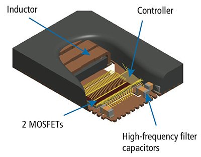
Altera’s Enpirion PowerSoC DC-DC converter family is a good example of a power module that incorporates an inductor. The EN23F2QI buck regulator, for instance, integrates MOSFET switches, small signal control circuits, compensation, and an inductor into a 12 x 13 x 3 mm QFN package (Figure 3).
For more detail: The Advantages (and Drawbacks) of DC-to-DC Voltage Converters with Integrated Inductors