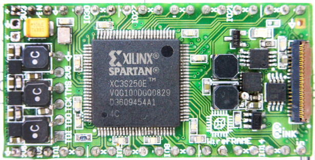
I have built a little FPGA board Xilinx xc3s250e called WireFrame. the board is only 50mm x 25 mm in size and it is possible to breadboard it. board also has 32MByte SDRAM, 4MByte serial Flash for storage. total 3 2A max each Switching regulator for Vcc I/O 3.3V (adjustable with regulator feed back resistors), VCCAUX 2.5 V and VCCINT 1.2v.
the first version of the board also had some switching boost circuit to generate various rails for E-ink displays. we don't need this feature for our current project. actually a little while back , I was working on project which interface a 6” E-ink display to a ARM CPU Running Linux. the over all Requirement was in such shape it was not possible directly interface the display to the Linux machine because of the way raw e-ink screen works.E-ink screen does not have any intelligent controller built-in it has only a few Row and column driver which make the whole thing work. so I worked a little FPGA solution to work as controller instead going for standard controller IC because of few reasons.
The board “WireFrame” has Xilinx XC3S250E at its core ,has 4MByte serial flash for bit-stream storage,32 MByte of SDRam and a small 25Mhz crystal oscillator (can be used FPGA's DCMs to multiply the clock upto hundreds of Mhz), total 3 2A each power regulator with maximum 6V input ,one regulator each For VccI/O 3.3V , VccAUX 2.5V and VccINT 1.2V. board completely breadboard-able , has two 19pin 0.1” pitch header to be inserted into breadboard. out of total 19 pins there are power input , all 3 regulator’s output, FPGA reset and FPGA I/O them self , few I/O are marked with capability of being configurable as differential pair.a six pin 2.5V JTAG header is separate for FPGA bit-stream download. board comes in very small size of only 50x25mm.
the Xilinx XC3S250E it has 250K logic blocks 73Kbit Distributed RAM bits , 360K block ram , 20 Dedicated Multipliers , 4 DCMs. we have used VQG100 package which is very small for such a big FPGA for the shake of small board size. With VQG100 package we got only total 66 I/O (including input only) lines , 30 differential lines. more details how the FPGA is configured to boot ,powered and connected to other peripheral please refer to the schematic.
The DRAM
we have used winbond w9825g6 4 M x 4 BANKS x 16 BITS SDRAM.The RAM is mounted on the bottom side of the board ,it is in TSOP II 54-pin, 400 mil Package
The Serial Flash
we have used MX25L3206E , 32Mega Bit , 4 Mega Byte of serial , flash to store bit stream file. it possible to use the Flash to store user Data, but it require some special care need to be taken , as ChipEnable pin of Flash is connected to done pin of the FPGA so after configuration finish the FLASH automatically get disabled , so to keep it enabled you need to short two smd header on the board to keep the FLASH always enabled, by this you will lose the facility of Done pin , means you on board configuration finish led will always be off. and there DRAM pins also multiplexed with Flash so you will not be able to access DRAM also.
I am an experienced technical writer holding a Master's degree in computer science from BZU Multan, Pakistan University. With a background spanning various industries, particularly in home automation and engineering, I have honed my skills in crafting clear and concise content. Proficient in leveraging infographics and diagrams, I strive to simplify complex concepts for readers. My strength lies in thorough research and presenting information in a structured and logical format.
This website uses cookies to improve your experience. We'll assume you're ok with this, but you can opt out if you wish.ACCEPTCheck Privacy Policy
Manage consent
Privacy Overview
This website uses cookies to improve your experience while you navigate through the website. Out of these, the cookies that are categorized as necessary are stored on your browser as they are essential for the working of basic functionalities of the website. We also use third-party cookies that help us analyze and understand how you use this website. These cookies will be stored in your browser only with your consent. You also have the option to opt-out of these cookies. But opting out of some of these cookies may affect your browsing experience.
Necessary cookies are absolutely essential for the website to function properly. This category only includes cookies that ensures basic functionalities and security features of the website. These cookies do not store any personal information.
Any cookies that may not be particularly necessary for the website to function and is used specifically to collect user personal data via analytics, ads, other embedded contents are termed as non-necessary cookies. It is mandatory to procure user consent prior to running these cookies on your website.