Continuing semiconductor scaling down to feature sizes of 7 nm is expected to yield further gains in performance, and lower power levels, but in IBM’s words, “[its] researchers had to bypass conventional semiconductor manufacturing approaches”. The finFET-style transistors in the demonstrator were constructed with silicon-germanium (SiGe) channels, and the lithography that defined them employed Extreme Ultraviolet (EUV) technology, “at multiple levels”. [That is, the use of EUV was not reserved for definition of a single critical part of the transistor structure.]
The announcement is of a demonstrator chip with working transistors; the company has not offered any insights as to what performance has actually been realised in the test chip, nor of any forecasts on when such as process might make the transition to production.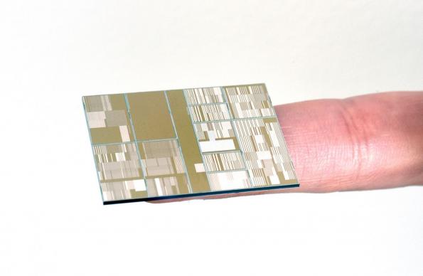
Microprocessors built in 22nm and 14nm technology power today’s servers, cloud data centres and mobile devices, and 10nm technology is well on the way to becoming a mature technology. The IBM Research-led alliance says it achieved close to 50% area scaling improvements over today’s most advanced technology [the company did not specify exactly what it regards that benchmark as being], introduced SiGe channel material for transistor performance enhancement at 7nm node geometries, process innovations to stack them below 30nm pitch and full integration of EUV lithography at multiple levels. These techniques and scaling could result in at least a 50% power/performance improvement for next generation mainframe and Power systems that will power the Big Data, cloud and mobile era.
For more detail: IBM shows working devices fabricated at 7nm node