1. Introduction
Problem
With the emergence of renewable energy sources, maintaining grid stability has become increasingly challenging. According to a 2018 study on consumer energy management, 68% of residential consumers, a 3% increase from 2016, express significant concern about climate change and their carbon footprints. Additionally, 7 in 10 businesses report that their customers are demanding a certain percentage of their electricity to come from renewable sources, marking a 9-point increase from 2017. This growing demand from consumers and businesses underscores the need for a greater reliance on renewable energy. However, renewable sources such as wind and solar are inherently unstable and difficult to predict in terms of energy output. Each new renewable source adds complexity to the balancing act between energy supply and demand, necessitating effective energy management systems.
Traditionally, energy balance has been the responsibility of utility companies. In response to these challenges, in 2015, the California Public Utilities Commission mandated that the state's investor-owned utilities adopt time-of-use (TOU) rates by 2019. Under this system, consumers are charged higher rates during peak demand hours and rewarded for reducing energy consumption during these periods. While TOU rates help alleviate strain on the power grid, they also result in increased costs for consumers. There is ongoing debate regarding the effectiveness of TOU rates compared to alternative methods of power consumption management, such as tiered rates, where consumers pay prices based on their usage relative to the overall average.
Solution
However, it is conceivable to achieve grid equilibrium primarily through demand-side management, all while incorporating financial incentives. Time of Use strategies all rely on consumers actively and consciously managing their own usage. Nevertheless, with our operational communication system, consumers may eventually have the option to allow their utilities to be efficiently regulated from the demand side.
The implementation of demand response systems necessitates substantial coordination of diverse loads drawing power from the same grid. By establishing a centralized communication method to reach loads across the grid, a utility company could enhance predictability in consumer-side demand, thereby reducing the overall required capacity and passing on economic benefits to participating consumers. Our objective is to design this communication system to adjust the effective duty cycle of multiple loads on the grid and synchronize demand to alleviate peak loads.
Visual Aid
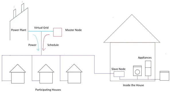
The diagram depicted above illustrates the envisioned utilization of our system within the power grid context. Power is transmitted from the source to the households along with a signal intended for interpretation by the Master Node. Upon interpretation, scheduling notifications are dispatched to the Slave Nodes situated in each participating household. Subsequently, each Slave Node regulates the power consumption of its associated appliances in accordance with the schedule provided. In the diagram, blue lines denote power transmission, red indicates scheduling data transmission, and purple signifies both.
High Level Requirements
1. Efficiently transmit data from the power source through the powerline (the virtual grid), enabling an n-bit signal to travel via a carrier wave to a receiver located at the load end.
2. Skillfully control the activation and deactivation of connected appliances according to schedules derived from received data transmissions.
3. Have the capability to adjust schedules in response to seasonal variations in demand. For instance, different schedules are necessary for Fall compared to Winter due to distinct demand patterns during these seasons.
2. Design
Block Diagram
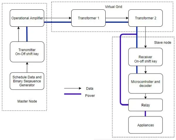
Figure 2: To ensure the effective functioning of our system, three subsystems are necessary: the Master Node, the Virtual Grid, and the Slave Node. The Master Node utilizes on-off shift keying and an amplifier to process scheduling data before transmitting it across the Virtual Grid. Upon reception at the Slave Node, the scheduling data is processed by a microcontroller, which then directs connected appliances based on the provided schedule. Any updated scheduling data sent to the Slave Node will accordingly adjust the commands issued by the microcontroller to the appliances.
Master Node: The primary control mechanism at the substation consists of a set of signals that will ultimately regulate all loads across the grid. This system also guarantees that there is sufficient power available on the grid to accommodate the cumulative demand of all the cycles it governs.
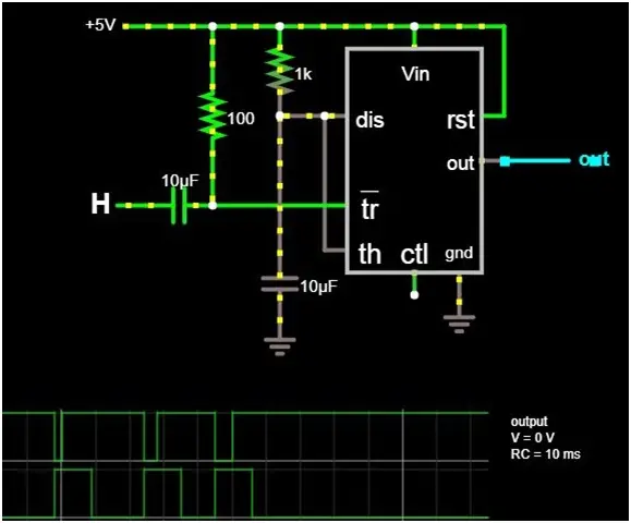
For the Schedule Data and Binary Sequence Generator, we utilize a binary sequence to modulate a carrier signal. The assignment of bits within this binary sequence is crucial as it represents data comprehensible to the microcontroller within the Slave Node. Each instance of a new schedule necessitates either the creation of a fresh binary sequence or an update to an existing one. Although our current approach involves simulating this data using a pulse generator, in the final design, the signals would be transmitted through a microcontroller.
Increasing the resistance would result in a wider pulse. For instance, using a 20k resistor would effectively double the pulse width. By adjusting this resistor, we can create a binary sequence for modulating a carrier signal.
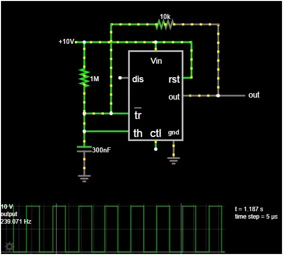
On-off shift keying (OOK) stands as the most basic form of amplitude shift keying modulation and will serve as our chosen technique for encoding a carrier wave signal with digital data.
In this method, a high-frequency carrier signal undergoes modulation with a binary sequence, generating a signal that mirrors the original carrier signal whenever the binary signal is at 1, and presents a constant signal level whenever the binary signal is at 0. This concept is depicted in the figure below. For the sake of simplicity, we will maintain a constant frequency and phase for the carrier signal.
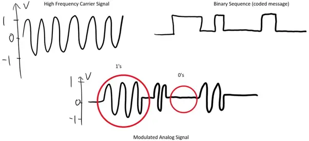
We need to define a time period, denoted as T, corresponding to the frequency that signifies 1 bit. This is crucial to distinguish the carrier wave, oscillating between -1 and 1, from the flatline segments of the modulated wave. For instance, if the peak-to-peak oscillation occurs over 1 second, we set 1 second equal to 1 bit. Assuming the initial flatline segments are 2 seconds, 1 second, and 3 seconds long respectively, our modulated signal would translate to 00111011000. With our digital code now represented in analog format, it becomes ready for transmission across the virtual grid.
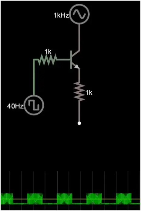
As depicted in the illustration, when the digital signal (a 40Hz square wave) provides a non-zero input, it triggers the transistor to enable the output of the carrier signal (a 1kHz AC source). In the absence of an input from the digital signal, the output is approximately -1V. Ideally, the output should be zero; however, due to some offsetting, we can observe the intended functionality of the modulator.
| Requirements (On-Off shift keying) | Verification |
| Correct modulation of carrier signal | Example: Scope both the carrier and the modulated signal and read “1011” and compare it to the input of the binary sequence generator |
- Transmitter: This component links with an amplifier, transmitting the modulated signal across the virtual grid. True to its name, it transfers data from the utility substation onto the grid.
| Requirements | Verification |
| Must send signal without detrimental distortion. | Example: Scope output of “1011” at the wire which goes into the operational amplifier, with 10% variances in pulse widths |
- Amplifier: The amplifier must achieve a gain of 20 V/V or higher without experiencing clipping. While resembling a parameter typically found in datasheets, it's important to highlight this requirement as issues often arise from amplifiers being incorrectly powered or connected, leading to non-functionality.
Virtual Grid: The route taken by our signals is analogous to that of an electric wire with minimal resistance, as we consider it in our design.
Transformers: In our block diagram, these transformers symbolize the step-up/step-down transformers employed in the grid. However, for our project, as we are simulating a virtual grid, these transformers won't be utilized. Instead, we'll opt for 1:1 isolating transformers..
| Requirements | Verification |
| All signals made by the system must be under 500 kHz by U.S. law. No radio waves in free space if unshielded wiring is used. | Measure signals at each electrical node and ensure there are no frequency components above 500 kHz |
Slave Node:
The receiver functions as an asynchronous demodulator, converting the incoming analog signal into a digital output compatible with the microcontroller. Illustrated in Figure 5, this module comprises a half-wave rectifier that channels a positive half output into a low-pass filter. The filter extracts the signal's envelope, transforming it into a digital format. Subsequently, the envelope is forwarded to a comparator to complete the digital signal conversion process.
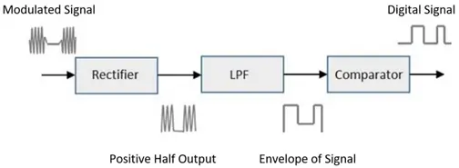
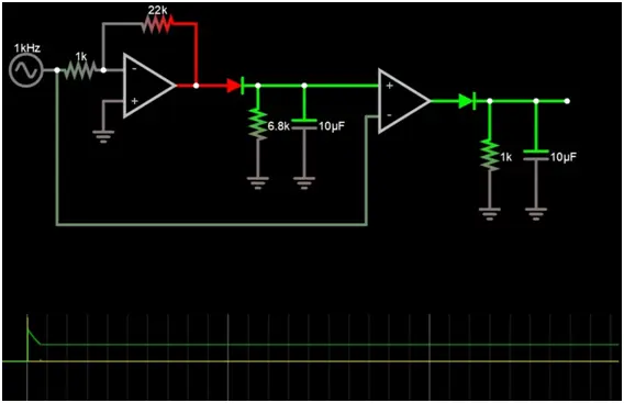
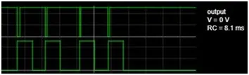
Figure 7 illustrates that the resultant output is a pure unit step, as the input remains unmodulated.
| Requirements | Verification |
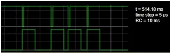
| Must decode the information from the transmitter correctly, at least in an ideal situation where the transmitted signal is perfect/directly in communication with the receiver. For example, if 1011 is transmitted, 1011 should be received. | Scope the output of the demodulator and the output of the transmitter simultaneously. The graphs should be very similar to within 5% rise and fall time delay.
Find correct values for resistors and capacitors to properly filter signals using these equations:
V ripple = Iload/fc V cap = V source e−t/RC
To minimize noise while having reasonable capacitor discharge times |
- Microcontroller: Essentially opens or closes the relay for the load based on initial binary sequence representing schedule commands being properly transmitted and received
The information transmitted across the virtual grid comprises an array of arrays. This setup essentially functions as a “broadcast” across the grid, making all device schedules accessible within this array. The following pseudocode provides a representation of this:
allSchedules = [A, B, C, D, E … ] // This array encompasses all schedules
B = [ deviceId = “B”, changeSchedule = true, newSchedule = [12pm: on, 1pm: off, default: off], currentTime = 12pm ] // This example depicts one of the subarrays. It contains scheduling details for a load identified by serial number “B.” Only the device with a matching serial ID of “B” will adhere to the instructions specified within array B. In this particular scenario, device B will adjust its schedule, receiving power from 12pm to 1pm, after which it will switch off and remain inactive until receiving further instructions.
| Requirements | Verification |
| Must store correct bit representations as intended by transmitter/receiver and properly control the relay switch with those signals. | Send a test input to the microcontroller and then view the output through 4 LEDs or a console. The 4 LEDs represent the next 4 hours of operation and LED on = power and LED off = no power.
The console command would just output a 4 bit array where 1 = power and 0 = no power
|
Relay: The switch operates based on microcontroller commands, enabling the connection or disconnection of power to a load (appliance). While it aligns with a “data sheet” parameter, it's crucial to highlight its role in controlling power to the appliance, marking the final step and achievement of the transmitted data word.
| Requirements | Verification |
| Must respond to a signal with no more than 5s delay. | Send a test input and measure the time it takes for the relay to react |
Tolerance Analysis and Feasibility
As our communication system operates on transmitting data from remote power sources to the connected devices, it's crucial to account for the transmission of higher frequency signals through power lines. Our primary hurdles lie in mitigating noise interference and deciphering signals affected by irregularities in power quality, such as incorrect voltage levels or additional frequency components. It's imperative to address variations in pulse width and filter characteristics, pivotal elements in achieving effective power line communication within our project's virtual grid.
Initially, we revisit Figure 3b, adjusting the resistance to 900 ohms (instead of the intended 1000 ohms) and the capacitance to 9 uF (instead of 10 uF), reflecting a 10% deviation for each component. Subsequently, we manually transmit a sequence of 4 bits.
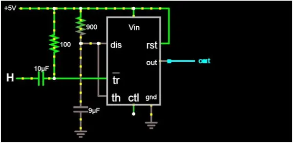
The cumulative impact of errors is evident, with a multiplicative effect. This results in an RC time constant for pulse width that is 19% shorter than initially planned, necessitating adjustments to ensure accurate data transmission. It underscores the importance of post-assembly measurements to ascertain the precise tolerance of the circuit. Subsequent design phases must accommodate inputs within a tolerance range of +/-(1-nm), where ‘n' represents the highest tolerance of any circuit element and ‘m' denotes the total contributing elements to the signal filters. Practically, this implies the receiver should be capable of decoding logical 1s that are 20% shorter or longer in width than those generated by the transmitter.
Although not visually apparent in the images, voltage levels may unpredictably deviate due to tolerance issues or parasitic components. It's reasonable to anticipate a potential 10% fluctuation in voltage levels. To mitigate this, high/low voltage cutoffs can be set up to 20% below the intended high analog voltage.
The active-low design of the binary sequence generator already accommodates varying pulse width inputs. However, the subsequent critical consideration lies in filtering, which is contingent upon resistor and capacitor tolerances. For the high pass filter crucial for our desired signal filtration, the cutoff frequency is determined by 1/(2*pi*R*C). Considering a 10% tolerance per component, the true cutoff frequency could be up to 23.5% higher or 17% lower than intended. Assuming a modulated signal frequency of 1000 Hz, setting the high pass filter to 806 Hz or lower accounts for the potential higher true frequency to prevent signal loss.
Feasibility
To substantiate the advantages of the system, it is beneficial to characterize the load profile from the power plant's perspective and simulate it by aggregating data from numerous residential units over the course of the year.
This simulation can be achieved through load profile generation using Python. Initially, import essential mathematical, plotting, and graphical libraries:
“`python
%matplotlib inline
import numpy as np
import pandas as pd
import matplotlib.pyplot as plt
import enlopy as el
“`
Next, specify the percentage of the week during which loads will operate on a typical “work day” (Monday to Friday, inclusive). Different load curves are applied for weekends, which are derived from separate tables. This parameter is referred to as the ‘workTime' variable.
workTime = .75 # 75% weekdays and 25% weekends
Load1 = el.gen_load_from_daily_monthly(monthlyLoad, dailyWorkingLoad, dailyNonWorkingLoad, Weight)
Load1.name = ‘firstHouse'
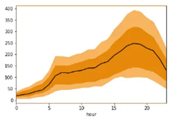
Load1.plot(figsize=(16,3), linewidth =.2, grid = False, perc_list=[[1,99], [25,75], 50], color='orange'));