
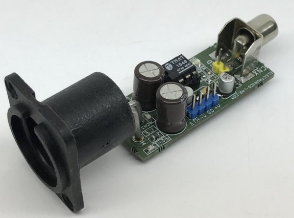
This audio-balanced line driver project enables to drive hundreds of feet in length of cables without becoming unstable The project is based on the THAT1646 chip, which is a new generation monolithic differential line driver that offers improved performance over conventional cross-coupled designs. Based on high performance, fully differential op-amp exhibits low noise and distortion, high slew rate, and wide output swing. Output is very stable when driving difficult loads, and output is short-circuit protected. The operating power supply is +/-15V DC, XLR, and RCA connector provided for output and input. D1, D2 are the Power LEDs, C7 decoupling capacitor, Ferrite Bead L1, L2, capacitor C6, C8, C9 take cares of RFI noise, Capacitors C5, and C10 acouple the common-mode feedback loop. This changes the loop operation from serving the common-mode output current at audio frequencies to serving the common-mode output voltage to 0 at DC. This results in much lower common-mode output offset voltage. D1 +VCC Power LED, D2 -VEE Power LED, CNX-J1 single-ended unbalanced audio input, CN3 Male XLR balanced audio output, CN1 power input, CN2 or J1-CNX audio input.
FEATURES
- Operating Power-Supply Nominal +/-15V DC (Dual) (Range +/-4V to +/-18V)
- Input Impedance 5Kohms
- Gain 6dB R-Load=100kOhms Per Output, 5.3 dB with 600 Ohms Load
- Gain Error 0.02dB
- DC Power Supply Rejection Ratio (PSSR) 107 dB
- Output Common-Mode Rejection Ration (CMMR) 65dB
- Output Signal Balance Ration 54dB
- THD+N (Balanced) VO=10V, R-Load=600Ohms, 20Hz-5Khz 0.0007 %, 20Khz=0.002%
- Output Noise Balanced 22Hz-20Khz -101dBu
- Maximum Output Level VO-max 27.5dBu
- Output Common-Mode Voltage Offset +/-3.5mV
- Output Voltage Swing, Positive (Without Load) VCC-2.2V
- Output Voltage Swing, Negative (Without Load) VEE+2.25V
- PCB Dimensions 48.62 x 19.67 mm
THAT1646 uses patented OutSmarts technology. Outsmarts is a dual feedback-loop design that prevents the excessive ground currents typical of cross-coupled output stages (CCOS) when clipping into single-ended loads. Chip has two individual negative-feedback loops to separately control the differential output voltage and common mode output currents, making the designs inherently more stable and less sensitive to component tolerances than common CCOSes. As a result, THAT’s topology prevents the loss of common-mode feedback that plagues common CCOS designs when clipping into single-ended loads. This avoids excessive ground currents that would otherwise upset power supplies and create additional distortion, even in adjacent channels.
Read more: AUDIO-BALANCED LINE DRIVER – UNBALANCED AUDIO TO BALANCED AUDIO CONVERTER