Intel's first product was not a processor, but a memory chip: the 31011 RAM chip, released in April 1969. This chip held just 64 bits of data (equivalent to 8 letters or 16 digits) and had the steep price tag of $99.50.2 The chip's capacity was way too small to replace core memory, the dominant storage technology at the time, which stored bits in tiny magnetized ferrite cores. However, the 3101 performed at high speed due to its special Schottky transistors, making it useful in minicomputers where CPU registers required fast storage. The overthrow of core memory would require a different technology—MOS DRAM chips—and the 3101 remained in use in the 1980s.3
This article looks inside the 3101 chip and explains how it works. I received two 3101 chips from Evan Wasserman and used a microscope to take photos of the tiny silicon die inside.4 Around the outside of the die, sixteen black bond wires connect pads on the die to the chip's external pins. The die itself consists of silicon circuitry connected by a metal layer on top, which appears golden in the photo. The thick metal lines through the middle of the chip power the chip. The silicon circuitry has a grayish-purple color, but it largely covered by the metal layer. Most of the chip contains a repeated pattern: this is the 16×4 array of storage cells. In the upper left corner of the chip, the digits “3101” in metal identify the chip, but “Intel” is not to be found.
Overview of the chip
The 3101 chip is controlled through its 16 external pins. To select one of the chip's 16 words of memory, the address in binary is fed into the chip through the four address pins (A0 to A3). Memory is written by providing the 4-bit value on the data input pins (D1 to D4). Four data output pins (O1 to O4) are used to read memory; these pins are inverted as indicated by the overbar. The chip has two control inputs. The chip select pin (CS) enables or disables the chip. The write enable pin (WE) selects between reading or writing the memory. The chip is powered with 5 volts across the Vcc and ground pins.
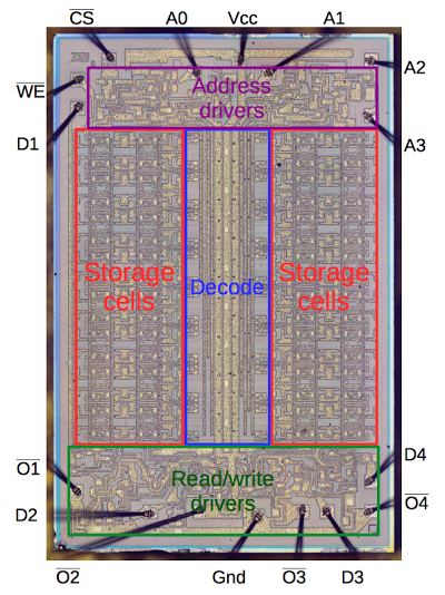
The diagram below shows how the key components of the 3101 are arranged on the die. The RAM storage cells are arranged as 16 rows of 4 bits. Each row stores a word, with bits D1 and D2 on the left and D3 and D4 on the right. The address decode logic in the middle selects which row of storage is active, based on the address signals coming from the address drivers at the top. At the bottom, the read/write drivers provide the interface between the storage cells and the data in and out pins.
Transistors
Transistors are the key components in a chip. The 3101 uses NPN bipolar transistors, different from the MOS transistors used in modern memory chips. The diagram below shows one of the transistors in the 3101 as it appears on the die. The slightly different tints in the silicon indicate regions that have been doped to form N and P type silicon with different semiconductor properties. The cross-section diagram illustrates the internal structure of the transistor. On top (black) are the metal contacts for the collector (C), emitter (E), and base (B). Underneath, the silicon has been doped to form the N and P regions that make up the transistor.
A key innovation of the 3101 was using Schottky transistors (details), which made the 3101 almost twice as fast as other memory chips.5 In the cross section, note that the base's metal contact touches both the P and N regions. You might think this shorts the two regions together, but instead a Schottky diode is formed where the metal contacts the N layer.6
Read more: Inside Intel’s first product: the 3101 RAM chip held just 64 bits


