
When working with discrete JFETs, designers may need to accommodate a large variation in device parameters for a given transistor type. A square-law equation is usually used as an approximate model for the drain-current characteristic of the JFET: ID=β(VGS−VP)2, where ID is the drain current, VGS is the gate-to-source voltage, β is the transconductance parameter, and VP is the gate pinch-off voltage. With this approximation, the following equation yields the zero-bias drain current at a gate-to-source voltage of 0V: IDSS=βVP 2, where IDSS is the zero-bias drain current.
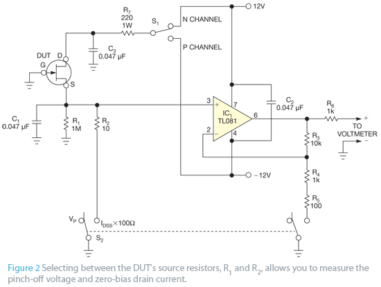 Figure 1 is a plot of this characteristic for N-channel JFETs showing the variation possible in a collection of devices. For example, the 2N4416A’s data sheet lists a pinch-off voltage of −2.5 to −6V, and the zero-bias drain current can range from 5 to 15 mA. You can observe the correlation between these two parameters across a sample of devices. The outer curves in the plot represent these extreme cases, and the center curve represents perhaps a typical case of a pinchoff voltage of −4V and a zero-bias drain current of 8 mA.
Although you can design around a certain amount of device variation for a mass-produced circuit, you sometimes need a tool to quickly characterize an assortment of discrete devices. This tool allows you to select a device that will optimize one circuit or perhaps to find a pair of devices with parameters that match reasonably well.
Figure 2 shows a simple test circuit for this purpose. Although the figure shows the JFET as an N-channel device, the JFET DUT (device under test) may be of either polarity, as selected by switch S1. An external voltmeter connects to the terminals on the right. Switch S2 selects two distinct measurement modes—one for the pinch-off voltage and another for the zero-bias drain current. In the pinch-off-voltage mode, the external voltmeter directly reads the pinch-off voltage; in the zero-bias-drain-current mode, the measured voltage is the zero-bias drain current across an apparent resistance of 100Ω.
For more detail: Simple circuit lets you characterize JFETs