memory

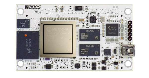
M100PFS – POLARFIRE RISC V SOC FPGA MODULE

M100PFS – POLARFIRE RISC-V SOC-FPGA MODULE

The M100PFS is based on the PolarFire SoC FPGA architecture by Microsemi and combines high-performance 64-bit RISC-V cores with outstanding FPGA technology. The platform integrates a hardened real-time, Linux capable, RISC-V-based MPU subsystem on the mid-range PolarFire FPGA family, bringing low power consumption, thermal efficiency and defence grade security to embedded systems. The RISC-V CPU

M100PFS – POLARFIRE RISC-V SOC-FPGA MODULE Read More »

Parallel Computing On Raspberry Pi 4B IoT Boards Made Easy

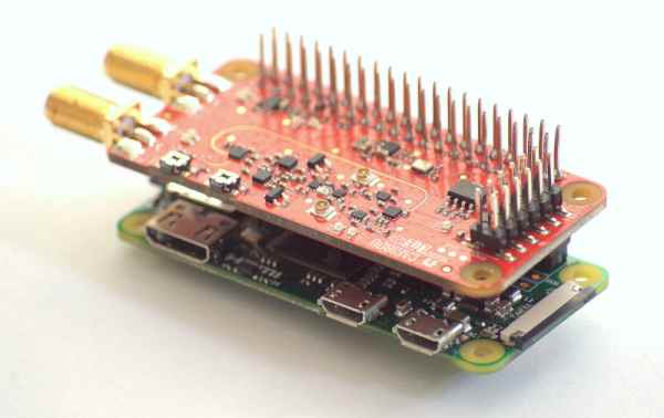
Parallel Computing On Raspberry Pi 4B+ IoT Boards Made Easy

Building and running a parallel code in C++17, implemented using Khronos CL/SYCL-model specification, on Raspberry Pi IoT boards. Our Goals… This project provides the useful guidelines, tips and tutorials for building a modern parallel code in C++17/2×0, implemented using CL/SYCL programming model, and running it on the next generation of Raspberry Pi 4B IoT boards,

Parallel Computing On Raspberry Pi 4B+ IoT Boards Made Easy Read More »

SAMSUNG UNVEILS 12 LAYER 3D TSV CHIP PACKAGING TECHNOLOGY

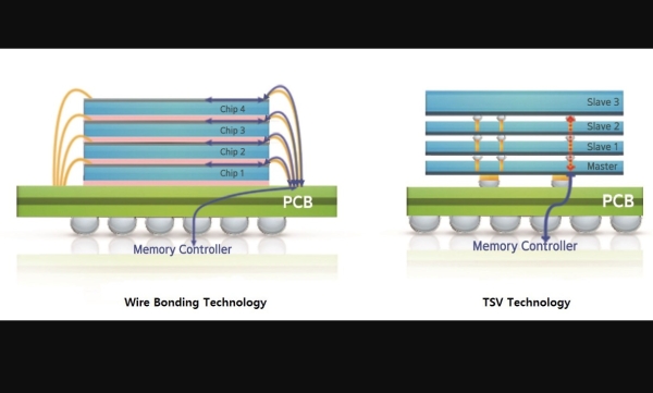
SAMSUNG UNVEILS 12-LAYER 3D-TSV CHIP PACKAGING TECHNOLOGY

An industry’s first, the 12-layer 3D-TSV (Through Silicon Via) technology developed by Samsung Electronics enables the stacking of 12 DRAM chips using more than 60,000 TSV holes, while maintaining the same thickness as current 8-layer chips. By Julien Happich @ eenewseurope.com Developed for the mass production of high-performance chips, the layered packaging technology requires pinpoint accuracy

SAMSUNG UNVEILS 12-LAYER 3D-TSV CHIP PACKAGING TECHNOLOGY Read More »

AI COMPUTE ACCELERATION STARTUP BUILDS THE LARGEST CHIP EVER FOR DEEP LEARNING APPLICATIONS

AI COMPUTE ACCELERATION STARTUP BUILDS THE LARGEST CHIP EVER FOR DEEP LEARNING APPLICATIONS

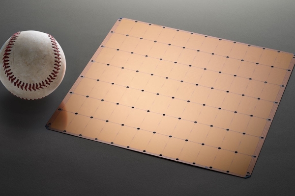
To meet the ever-increasing computational demands of AI, California based AI startup, Cerebras Systems, just recently unveiled its very first announced element claimed to be the most massive AI chip ever made. With an astounding measurement of 46,225 mm2 (up to 56.7 times more than the largest graphics processing unit) and more than 1.2 trillion transistors, the Wafer-Scale Engine

AI COMPUTE ACCELERATION STARTUP BUILDS THE LARGEST CHIP EVER FOR DEEP LEARNING APPLICATIONS Read More »

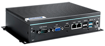
NEW KONTRON COME M4AL10 E2 MODULE

NEW KONTRON COME-M4AL10 (E2) MODULE

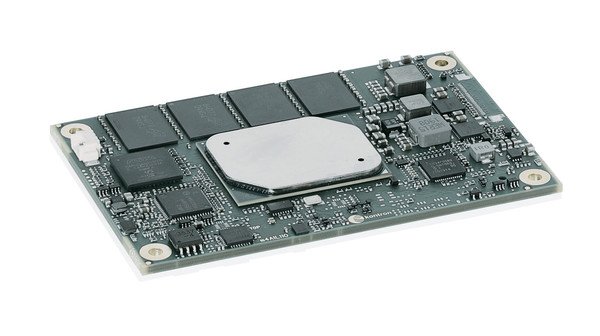
The COMe-m4AL10 (E2) is ideally suited for use in industrial IoT and Industry 4.0 applications Kontron has introduced its new COMe-m4AL10 (E2) module. The module is available with either Intel Atom®, Intel® Pentium® or Intel® Celeron® processors of the latest 5th generation. With dimensions of only 84 mm x 55 mm, it is an ideal solution for space-limited applications; furthermore

NEW KONTRON COME-M4AL10 (E2) MODULE Read More »

WORLD’S LARGEST FPGA BOASTS 9 MILLION SYSTEM LOGIC CELLS

WORLD’S LARGEST FPGA BOASTS 9 MILLION SYSTEM LOGIC CELLS

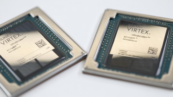
Xilinx has expanded its 16nm Virtex UltraScale+ family to include what it claims to be the world’s largest FPGA, the Virtex UltraScale+ VU19P. By Julien Happich @ www.eenewseurope.com With 35 billion transistors, the VU19P provides the highest logic density and I/O count on a single device ever built, enabling emulation and prototyping of tomorrow’s most advanced

WORLD’S LARGEST FPGA BOASTS 9 MILLION SYSTEM LOGIC CELLS Read More »

Scroll to Top