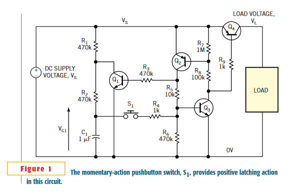
When you first apply the supply voltage, VS, all four transistors are off, and capacitor C1 charges via R1 and R2 until its voltage, VC1, is equal to VS. The circuit is now in its off, or unlatched, state, and the load voltage, VL, is 0V. A momentary closure of the pushbutton switch, however, causes C1 to dump its charge into the base of Q3, which conducts and furnishes bias for Q2 and Q4, which both turn on. Q2 now provides base bias for Q3 via R5, and also for Q1 via R3. The circuit is now in its on, or latched, state and remains that way even though S1 is open. The load is now energized, and VL is roughly equal to VS. Transistor Q1 is now saturated, causing C1 to discharge via R2 such that VC1 falls to a few tens of millivolts (Q1‘s collector-emitter saturation voltage). Another momentary closure of the pushbutton switch couples this low voltage to Q3‘s base, turning it off. As a result, all four transistors turn off, and the circuit reverts to its off, or unlatched, state. The load is now de-energized, and VL falls to 0V. Because Q1 is now off, C1 begins to charge again via R1 and R2, such that another momentary closure of S1 latches the circuit on again.
Timing capacitor C1, acting with R1 and R2, provides debouncing for the pushbutton switch, such that contact bounce has no effect on the desired latching function. Without the RC time delay, the circuit would “chatter” on and off each time you pressed the pushbutton switch and would end up in an indeterminate state. Although Figure 1 shows a value of 1 µF, other values may be more suitable for a particular application, so prepare to experiment. None of the resistor values is particularly critical, and the values shown in Figure 1 are fairly optimal for a supply voltage of approximately 1 to 1.5V—in other words, a single cell. At higher voltages, the resistor values should increase proportionally, although you should hold R2 and R4 constant at approximately 470 and 1 kΩ, respectively. Keeping the R2-C1 time constant fixed at a few hundred milliseconds ensures that the time taken to discharge the capacitor is not excessive; otherwise, once the circuit has been latched, there may follow an unacceptable delay before it can be unlatched. Resistor R4 limits the current flowing from C1 into Q3‘s base to a safe level; its value should be fairly small to ensure that R5 and R6 do not distort the voltage appearing at Q3‘s base when the switch closes.
You should size resistor R1 according to the supply voltage you use. For a given value of R2, R1 determines the time it takes VC1 to rise toward VS immediately after the circuit has been unlatched. In other words, R1‘s value determines the time needed to “prime” the circuit to make it ready to be latched on again. If R1 is too large, it becomes impossible to latch the circuit on soon after it has been unlatched. On the other hand, if R1 is too small, it may impose an unacceptable current drain on VS when the circuit is latched on. Furthermore, for a particular value of VS, R1 should be large enough to ensure that VC1 does not rise too quickly after the circuit has been unlatched, or it could turn the latch back on again before the switch has opened. You may need some experimentation to determine the optimum value for R1, but with C1=1 µF and R2=470 kΩ, the test circuit performed well with a value of approximately 470 to 680 kΩ at VS=1V and approximately 4.7 MΩ at VS=10V.
Transistors Q1 to Q3 can be any small-signal types with good current gain (moderate to high forward current gain). Power switch Q4 should have low VCE(SAT) to ensure most of the supply voltage is delivered to the load when the circuit is latched. You should select resistor R9 to furnish plenty of base drive for Q4; the value depends mainly on VS, on the load current, and on Q4‘s saturated current gain. The circuit provides an inexpensive way of deriving a latching function from a momentary pushbutton, and, like a mechanical latching switch, the quiescent (unlatched) current drain is zero.
For more detail: Latching power switch uses momentary-action pushbutton

