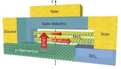
As Tomioka notes, the materials and type of architecture currently used in creating small consumer electronic devices is rapidly reaching a threshold upon which a tradeoff will have to be made—smaller transistors or more power requirements—this is because of the unique nature of FETs, shortening the channel they use requires more power, on a logarithmic scale. Thus, to continue making FETs ever smaller and to get them to use less power means two things, the first is that a different channel material must be found, one that allow high switch-on currents at low voltages. The second is a way must be found to lower the voltage required for the FETs.
Researchers have made inroads on the first requirement, building FETs with metal-oxide-semiconductor materials, for example. The second has proved to be more challenging. In this latest effort, the researchers looked to tunneling to reduce voltage demands, the results of which are called, quite naturally, tunneling FETs or TFETs—they require less voltage because they are covered (by a gate stack) and work by transporting a charge via quantum-tunneling. The device the team built is based on a 2D bilayer of molybdenum disulfide and bulk germanium—it demonstrated a negative differential resistance, a marker of tunneling, and a very steep subthreshold slope (the switching property associated with rapid turn-on) which fell below the classical theoretical limit.

