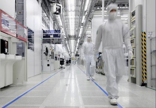
“The new fabrication plant in Pyeongtaek constitutes an important part of our vision to establish a globally balanced semiconductor fabrication network that further solidifies our strong global presence,” Jim Elliott, corporate vice president, Samsung Semiconductor told EE Times. “The plant will play a key role in our future business initiatives, as we continue to invest in areas that contribute much towards our industry leadership.”Samsung reported that its smartphone sales were slumping 20 percent in the fourth quarter of 2014, while its semiconductor sales surged 50 percent. Samsung has since been reported to have surged back in smartphone sales in the first quarter of 2015, however its semiconductor division is still outpacing its smartphones potentially making its investment in a 10 nanometer fab a smart (if expensive) move.
For more detail: Samsung Building World’s Most Expensive Fab for 10-Nanometer FinFETs

