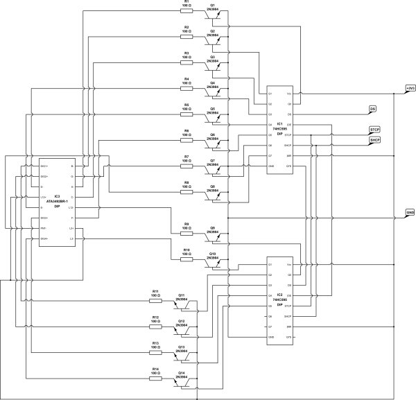
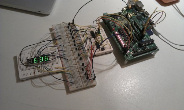
A serial-to-parallel shift register (or SIPO: Serial In Parallel Out) lets you take a sequence of signals on one output, and split them up into several separate outputs. For example, if you don’t have enough GPIO pins on your Raspberry Pi, Arduino, or other computer/microcontroller, you can use a shift register to add more.
In this post, I’ll be looking at the 74HC595, which is an 8-bit SIPO IC (i.e. it gives you 8 outputs). The advantage of this chip over some dedicated port expanders is that it doesn’t require a complex protocol like I2C or SPI, and it doesn’t need a particular clock speed. That means you can control it with pretty much any digital output channels, and it’s very easy to write simple software to communicate with it.
What does a shift register do?
In general, a shift register is a memory buffer which you write to and/or read from sequentially, depending on the application.
In the case of a serial-to-parallel shift register, you push data onto the beginning of the register, one bit at a time. Each time you do that, the existing data shuffles along to make room. Typically, you keep going until you’ve filled up the register, and then trigger a transfer.
The transfer copies all the data in the shift register over into a separate storage register. This will usually be connected to a series of outputs which all get updated simultaneously. This allows the outputs to hold the current values steady while you re-fill the shift register with the next block of data. You then trigger another transfer to update the outputs, and so on.
This makes it great for expanding outputs from something like a Raspberry Pi or Arduino. You use 3 of your device’s output pins to give data in serial to the register. It gets converted to parallel, letting you treat it as though you’ve got 8 or 16 (or more) individual output pins. It’s inevitably slower than having actual output pins, but effective for many purposes.
One of the great things about these components is that you can ‘daisy-chain’ them together. When you push a bit on to the shift register, the last bit has nowhere to go when everything else shuffles along. This means it usually just gets discarded. However, you can actually redirect it to the input for a second shift register, effectively doubling the output capacity. As long as you’ve got enough power, there’s nothing stopping you from daisy-chaining more, although the longer your chain the slower the updates will be.
How do you control the shift register?
The 74HC595 is controlled by a data input pin (DS), a shift clock pin (SHCP or SRCLK), and a storage clock pin (STCP or RCLK). They are all active high. In the case of the clock pins, you’ll need to make sure they’re pulled properly low (not floating) in between clock pulses, otherwise you’ll get odd behaviour.
When you want to move data onto the register, first set the data input pin (DS) high or low, representing the bit you want to send (i.e. 1 or 0). After that, briefly set the shift clock pin (SHCP) high, and then bring it back to low. Repeat this process as many times as you need to get data where you want it on the register (typically 8 times to fill a single register).
When you want to copy data to the output register, briefly pulse the storage clock pin high, then bring it back to low. (You’ll need to pull the Output Enable (OE) low as well, although as noted below I keep it held low at all times.)
And that’s it! The device is capable of fairly high speeds, so you can whizz quite a bit of data through. Bear in mind that the outputs aren’t capable of handling much load though, so remember to use transistors or similar if you want to power other devices directly.
Pin connections
Be careful of voltages when connecting the shift register to a device. The 74HC595 can work with a range of voltages, including 3.3v for Raspberry Pi, and 5v for most Arduinos. However, check your datasheets! In particular, watch out for the 74HCT595 (notice the “T” in there!). It will probably not operate properly at 3.3v.
The supply (Vcc) and ground (GND) pins are hopefully obvious — hook those up to your power supply and ground lines.

The Master Reset (MR) pin should be held high most of the time (e.g. by bridging it to Vcc). If this pin is pulled low then it will reset the entire shift register (basically filling it with 0’s). You can control this line from your device as well if you want, or connect it to a central reset circuit.
I usually prefer to hold the Output Enable (OE) pin low (e.g. by bridging it to GND). This keeps the storage register connected to the output pins at all times. If you let it go high then the output pins will float. This could have an odd effect on whatever is connected to the outputs, unless you setup circuitry to detect it.
If you’re only using a single shift register, you can leave the serial output pin unconnected (usually labelled Q7S, or sometimes Q7′).
Finally, hook up the output pins to whatever components you want to control (Q0 to Q7).
For more detail: What is a serial-to-parallel shift register


