
How can you count bits in hardware? In this article, I reverse-engineer the circuit used by the ARM1 processor to count the number of set bits in a 16-bit field, showing how individual transistors form multiplexers, which are combined into adders, and finally form the bit counter. The ARM1 is the ancestor of the processor in most cell phones, so you may have a descendent of this circuit in your pocket.
ARM is now the world's most popular instruction set but it has humble beginnings. The original ARM1 processor was designed in 1985 by a UK company called Acorn Computer for the BBC Micro home/educational computer. A few years later Apple needed a low-power, high-performance processor for its ill-fated Newton handheld system and chose ARM.[1] In 1990, Acorn Computers, Apple, and chip manufacturer VLSI Technology formed the company Advanced RISC Machines to continue ARM development. ARM became very popular for low power applications (such as phones) and now more than 50 billion ARM processors have been manufactured.
One way ARM processors increase performance is through block data transfer instructions, which efficiently copy data between on-chip registers and memory storage.[2] These instructions can transfer any subset of ARM's 16 registers in a single instruction. The desired registers are specified by setting the corresponding bits in a 16-bit field in the instruction. To implement the block transfer instructions, the ARM requires two specialized circuits. The first circuit, the bit counter, counts the number of bits set in the register select field to determine how many registers are being transferred.[3] The second circuit, the priority encoder, scans the register select field and finds the next set bit, indicating which register to load/store next.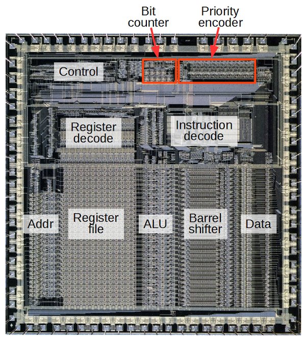
These two circuits are highlighted in red in the ARM1 die photo above. As you can see, the circuits take up a significant fraction of the chip (about 3%), but the chip designers felt the performance gain from block transfers was worth the increase in chip size and complexity. This article explains the bit counter, and I plan to describe the priority encoder later.
Zooming in on the bit counter reveals the circuit below. It looks like a jumble of lines, but by examining it carefully, you can get an understanding of what is going on. The remainder of the article explains how a special type of circuitry called pass transistor logic is used to build a multiplexer — a circuit that selects one of its two inputs. The multiplexers are used to form logic gates, which are then combined to form a full adder, which adds three bits. Finally, the adders are combined to create the bit counting circuit. If you're not familiar with digital logic or the ARM processor, you might want to start with my earlier article on reverse-engineering the ARM1 for an overview.
Pass transistors and transmission gates
The bit counter is built from a type of circuitry called pass transistor logic. Unlike normal logic gates, pass transistor logic switches the inputs themselves to pass an input directly to the output. Pass transistors are used because sums (i.e. XORs) are inconvenient to generate with standard logic and can be generated more efficiently with pass transistor logic.
The ARM1 chip, like most modern chips, is built from a technology called CMOS. The C in CMOS stands for complementary because CMOS circuits are built from two complementary types of transistors. NMOS transistors switch on when the control signal on the gate is high, and can pull the output low. PMOS transistors are opposite; they switch on when the gate's control signal is low, and can pull the output high. Combining an NMOS transistor and a PMOS transistor in parallel forms a transmission gate. If both transistors are on, the input will be passed to the output whether it is low or high. If both transistors are off, the input is blocked. Thus, the circuit acts as a switch that can either pass the input through to the output or block it.
The diagram below shows two transistors (circled) connected to form a transmission gate. The upper one is NMOS and the lower one is PMOS. On the right is the symbol for a transmission gate. Note that because the transistors are complementary, they require opposite enable signals.
Building the bit counter from adders
The bit counter takes 16 bit inputs and generates a 4-bit count as output, using adders as building blocks. The flow chart below shows how it operates, with data flowing from top to bottom. Each box is an adder, with carry (C) and sum (S) outputs. Boxes are colored according to which bit of the sum they are computing: red for the 1's bit, green for the 2's bit, blue for the 4's bit and purple for the 8's bit. Each box passes its sum output down and passes its carry to the left.
Overall, the process is similar to long addition if you could just add three digits at a time. You compute partial sums, then add up those sums, and so forth until all the sums are added up. Then the carries need to be added up, along with the sums of those carries, and so forth. If there are carries from those digits, they need to be added up, until finally everything has been added.
The first step of counting the bits is to add each triple of bits with a full adder, generating a two bit count (0, 1, or 2). Inconveniently, since the sixteen input bits aren't divisible by 3, one bit is left over and is handled separately. Next, the five partial sums are added by more adders (red). As carries are generated, they also get added (green). Carries from the carries are also added (blue). In the final step, two-input half adders[8] compute the sum output; these half adders are simpler than the three-input full adders.[9]
Notes and references
[1] An interesting interview with Steve Furber, co-designer of the ARM1, explains how ARM achieved low power consumption. Acorn wanted to use a low-cost plastic package for the chip, but it could only handle 1 Watt. The designers didn't have good tools for estimating power consumption, so they were conservative in their design and the final power consumption was way below the target, just 1/10 Watt. In addition, ARM1 had a simple RISC (Reduced Instruction Set Computer) design, which also reduced power consumption: ARM1 had about 25,000 transistors compared to 275,000 in the 80386 which came out the same year. Thus, the low power consumption of ARM that led to its wild success in mobile applications was largely accidental.
[2] ARM's block data transfer instructions are called STM (Store Multiple) and LDM (Load Multiple), storing and loading multiple registers with one instruction. These instructions don't exactly fit the RISC processor philosophy since they are fairly complex and perform many memory accesses, but the ARM designers took the pragmatic approach and implemented them for efficiency. These instructions can be used for copying data or for stack push/pop, saving registers in a subroutine call or interrupt handler. Note that these instructions are not implemented in microcode, but in hardware that steps through the registers and memory.
[3] It's not obvious why a bit counter is required at all. You'd think the chip could just store registers until it's done, without knowing the total count. The unexpected answer is that LDM/STM always start with the lowest address working upwards. For example, if you're popping 4 registers off the stack with LDM, you'd expect to start at the top of the stack and work down. Instead, the ARM pulls registers out of the middle of the stack: it starts four words from the top, pops registers in reverse order going up, and then updates the stack pointer to the bottom. The results are exactly the same as popping from the top, just the memory accesses are in the reverse order. (The STM instruction is explained in detail on the ARMwiki.) Thus, the bit counter is needed to figure out how far down to jump in memory at the start of the instruction.
For more detail: Reverse engineering the silicon in the ARM1 processor