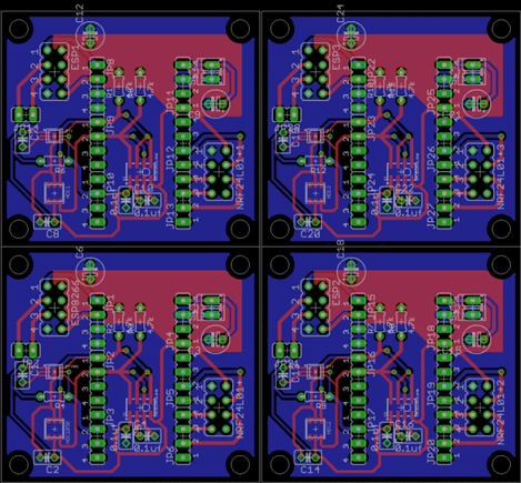
I have been working with Eagle for quite some time but never really got a PCB manufactured. almost all the time i used the toner transfer method to make homebrew PCBs. But then i took a project in which i had to use SMD components and i could no longer use toner transfer method because of the limits on resolution of the Laser printer.
Time had come for “properly” designing and generating “Gerber files”. When you are using toner transfer then there isn’t really a need to go into minute details of every layer as you know what you want exactly, but this approach dosen’t work with the manufacturers. Hence you have to take a lot of precautions and understand what exactly you are doing.
Till designing is okay for most of us. But then i needed to “Panelize” and then create the “Gerber” files.
PANELIZE
This is fairly easy to do. Just save your .brd and .sch files after you are done with the design. After that in the same folder create a new .brd file by doing File -> Your Project -> New -> Board
Now just save this board file without adding anything to it and name it as “project_name_panel.brd”. After that open your project and select the whole board then click on the “copy” icon. After that browse to your panel board file and then click on “Paste” icon. The whole board would be copied. Similarly you can copy “Different” board files(from different projects) into a SINGLE panel board file.
This step is NOT yet complete. Because of what you did just now Eagle will rename the component name so that no two components have the same name. So even if you are not copying a different board but making multiple copies of a single board the names of the components will be changed.
Notice the capacitor on the top in all the boards. They all have different names although they are the same.
Why ? Once the copy is placed on the board, Eagle automatically changes the part names to avoid duplication. Normally this is not a problem, but when you want to panelize a design you want all the panels to come out exactly the same. Some of you might be fine with this but some of you might not be. This especially becomes a nuisance if the board is of moderate to high complexity and has a lot of components. For that we run the “panelize.ulp” ULP. There are two ways to do that –
- File-> Run ULP -> From the window scroll down and choose “panelize.ulp”
- Tools -> Panelize -> Execute
You can see that the part names are still automatically corrected by Eagle (bad for us) but the original part names (in yellow) are all preserved (yay!). Now the only thing left is to tell the CAM processor that we want to export the newly created layer (with the same component names) rather than the original ones. This is how we get the FAB houses to print the same part names on the silk screen !!. We do that in the CAM settings page while running the CAM job OR we can directly edit the cam files!!
GERBER FILES generation
For that we need to run the CAM processor for generating the Gerber files. I had no idea how to do that. So i searched the net for resources and honestly it was of little help. I definitely learnt a few things but i got more confused. There were quite a few “custom” gerber generating files form Sparkfun and other individuals/institutions. And then there were videos that showed completely different (and possibly outdated) stuff. Then i found that Eagle itself has cam files for generating gerbers. After spending quite some time on it and understanding the steps in the video i thought lets just READ these cam files. So i read the cam files of Eagle and Sparkfun and then i had that moment of epiphany 😀 !. I understood everything properly.
If you open the “gerb274x.cam” in eagle->cam->gerb274x.cam you will notice that its not that overwhelming as you apparently thought it might be.
In a summary it has 5 or more sections(5 if it is the original one and more or less if it is a third party custom gerber generation cam file).
SECTION NAME Layer Numbers Layer Names Comment 1st Component Side 1,17,18 Top, Pads, Vias Do Not Change 2nd Solder Side 16,17,18 Bottom, Pads, Vias Do Not Change 3rd Silkscreen Side(Top) 20,21,25 Dimention,tPlace,tNames You can change
The Silkscreen part is a flexible one, it depends on what you decide. So after panelizing you should edit the original to 125 i.e” _tNames” layer. OR if you also want to have a silkscreen on the bottom side then you should have layer 126 i.e “_bName” too. Apart from that you can choose any other layer too like dimension layer(21) depending on your needs. So decide carefully what do you want.
4th Solder Stop Mask(Component side) 29 tStopSolder Do Not Change 5th Solder Stop Mask(Solder side) 30 bStopSolder Do Not Change
What are solder masks ? Solder mask or solder stop mask or solder resist is a thin lacquer-like layer of polymer that is usually applied to the copper traces of a printed circuit board (PCB) for protection against oxidation and to prevent solder bridges from forming between closely spaced solder pads.
For more detail: Panelizing and Gerber Generation in Eagle


